Light-Emitting Element, Display Device, Electronic Device, and Lighting Device

a technology of light-emitting elements and electronic devices, which is applied in the direction of light-emitting devices, semiconductor devices for light sources, organic semiconductor devices, etc., can solve the problems of difficult design of light-emitting materials that meet these two requirements, and achieve the effect of reducing driving voltage and increasing luminous efficiency

Pending Publication Date: 2017-01-12
SEMICON ENERGY LAB CO LTD
View PDF5 Cites 155 Cited by
  • Summary
  • Abstract
  • Description
  • Claims
  • Application Information

AI Technical Summary

Benefits of technology

[0012]In a light-emitting element containing a thermally activated delayed fluorescent emitter and a light-emitting material, it is preferable that c

Problems solved by technology

Among light-emitting elements containing phosphorescent materials, a light-emitting element that emits blue light in particular has yet been put into practical use because i

Method used


Image

  • Light-Emitting Element, Display Device, Electronic Device, and Lighting Device
  • Light-Emitting Element, Display Device, Electronic Device, and Lighting Device
  • Light-Emitting Element, Display Device, Electronic Device, and Lighting Device

Examples


embodiment 1

[0093]In this embodiment, a light-emitting element of one embodiment of the present invention will be described below with reference to FIGS. 1A to 1C, FIGS. 2A and 2B, and FIGS. 3A to 3C.

[0094]First, a structure of the light-emitting element of one embodiment of the present invention will be described below with reference to FIGS. 1A to 1C.

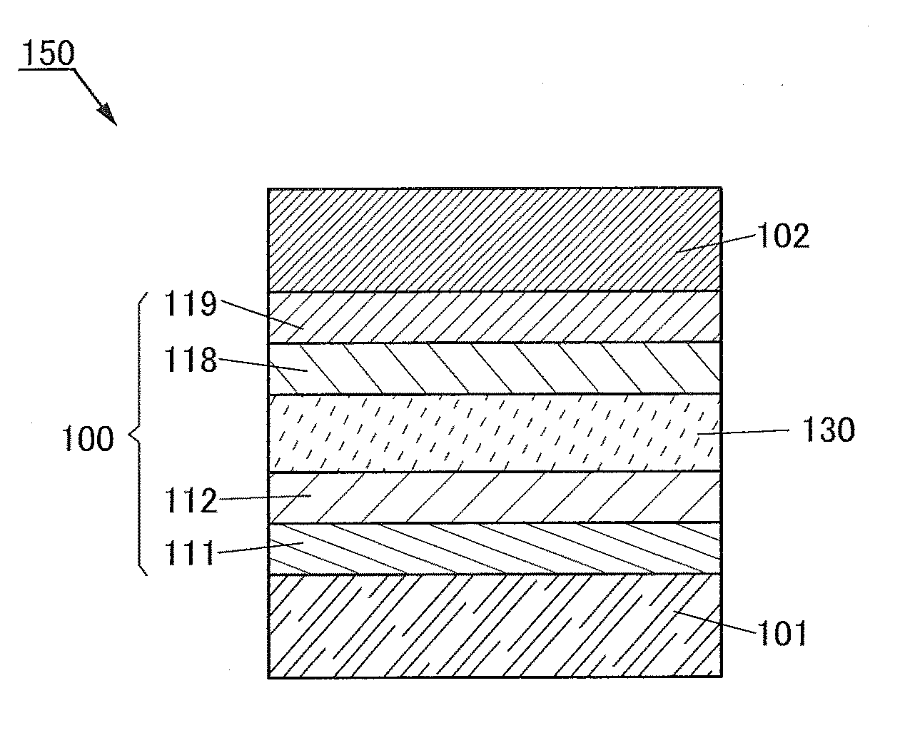
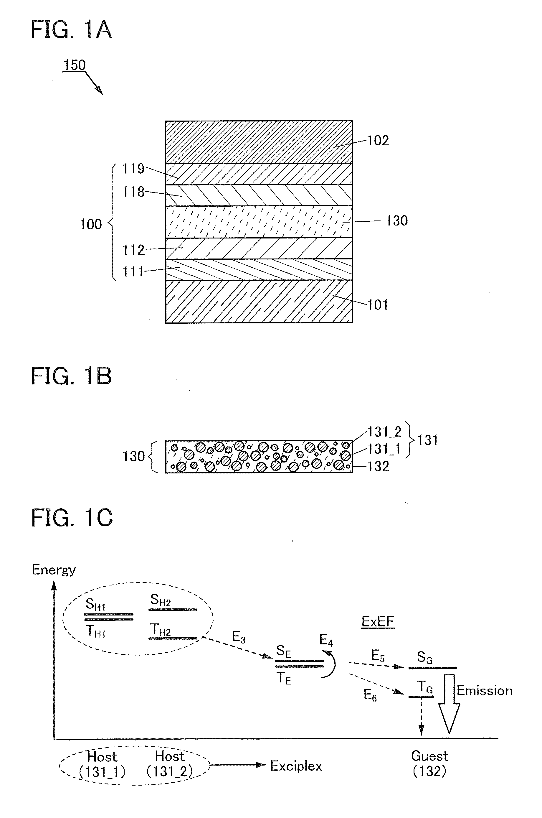
[0095]FIG. 1A is a schematic cross-sectional view of a light-emitting element 150 of one embodiment of the present invention.

[0096]The light-emitting element 150 includes a pair of electrodes (an electrode 101 and an electrode 102) and an EL layer 100 between the pair of electrodes. The EL layer 100 includes at least a light-emitting layer 130.

[0097]The EL layer 100 illustrated in FIG. 1A includes functional layers such as a hole-injection layer 111, a hole-transport layer 112, an electron-transport layer 118, and an electron-injection layer 119, in addition to the light-emitting layer 130.

[0098]Although description is given assuming that the ele...

embodiment 2

[0225]In this embodiment, a light-emitting element having a structure different from that described in Embodiment 1 and light emission mechanisms of the light-emitting element are described below with reference to FIGS. 4A to 4C. In FIG. 4A, a portion having a function similar to that in FIG. 1A is represented by the same hatch pattern as in FIG. 1A and not especially denoted by a reference numeral in some cases. In addition, common reference numerals are used for portions having similar functions, and a detailed description of the portions is omitted in some cases.

[0226]FIG. 4A is a schematic cross-sectional view of a light-emitting element 152 of one embodiment of the present invention.

[0227]The light-emitting element 152 includes a pair of electrodes (an electrode 101 and an electrode 102) and an EL layer 100 between the pair of electrodes. The EL layer 100 includes at least a light-emitting layer 140.

[0228]Note that the electrode 101 functions as an anode and the electrode 102 f...

embodiment 3

[0289]In this embodiment, light-emitting elements having structures different from those described in Embodiments 1 and 2 and light emission mechanisms of the light-emitting elements are described below with reference to FIGS. 5A to 5C and FIGS. 6A and 6B. In FIGS. 5A to 5C and FIGS. 6A and 6B, a portion having a function similar to that in FIG. 1A is represented by the same hatch pattern as in FIG. 1A and not especially denoted by a reference numeral in some cases. In addition, common reference numerals are used for portions having similar functions, and a detailed description of the portions is omitted in some cases.

[0290]FIG. 5A is a schematic cross-sectional view of a light-emitting element 250.

[0291]The light-emitting element 250 illustrated in FIG. 5A includes a plurality of light-emitting units (a light-emitting unit 106 and a light-emitting unit 108 in FIG. 5A) between a pair of electrodes (the electrode 101 and the electrode 102). Any one of the plurality of light-emitting ...


PUM

PropertyMeasurementUnit
Energyaaaaaaaaaa
Energyaaaaaaaaaa
Energy levelaaaaaaaaaa

Abstract

A light-emitting element containing a light-emitting material with high luminous efficiency is provided. The light-emitting element includes a host material and a guest material. The host material includes a first organic compound and a second organic compound. In the first organic compound, a difference between a singlet excitation energy level and a triplet excitation energy level is larger than 0 eV and smaller than or equal to 0.2 eV. The HOMO level of one of the first organic compound and the second organic compound is higher than or equal to that of the other organic compound, and the LUMO level of the one of the organic compounds is higher than or equal to that of the other organic compound. The first organic compound and the second organic compound form an exciplex.

Description

TECHNICAL FIELD[0001]One embodiment of the present invention relates to a light-emitting element, or a display device, an electronic device, and a lighting device each including the light-emitting element.[0002]Note that one embodiment of the present invention is not limited to the above technical field. The technical field of one embodiment of the invention disclosed in this specification and the like relates to an object, a method, or a manufacturing method. In addition, one embodiment of the present invention relates to a process, a machine, manufacture, or a composition of matter. Specifically, examples of the technical field of one embodiment of the present invention disclosed in this specification include a semiconductor device, a display device, a liquid crystal display device, a light-emitting device, a lighting device, a power storage device, a storage device, a method of driving any of them, and a method of manufacturing any of them.BACKGROUND ART[0003]In recent years, res...

Claims


Application Information

Patent Timeline
IPC IPC(8): H01L51/00H01L27/32H01L51/50
CPCH01L51/0051H01L51/5016H01L27/322H01L51/0077H01L2251/5384H01L51/0072H01L51/0071H01L51/0073H01L51/0067H10K59/38H10K59/40H10K85/113H10K50/11H10K2101/40H10K50/12H10K85/631H10K85/654H10K85/6576H10K85/6572H10K85/342H10K2101/10H10K2101/90H10K2101/30H10K2101/20F21Y2115/15H10K50/14
Inventor SEO, SATOSHIOHSAWA, NOBUHARU
Owner SEMICON ENERGY LAB CO LTD
Why Eureka
Try Eureka