Two-dimensional heterostructure materials

Active Publication Date: 2017-01-26
UT BATTELLE LLC
View PDF2 Cites 25 Cited by
  • Summary
  • Abstract
  • Description
  • Claims
  • Application Information

AI Technical Summary

Benefits of technology

[0009]A method, article of manufacture and system are provided for creating new compositions of matter. In a two dimensional material comprising a first composition of matter, lateral heterojunctions may be fabricated by first specifying a lithographic pattern for masked and exposed areas over the two dimensional material. A mask, for example SiO2 thin film, may then be deposited onto a planar surface of the two dimensional material in selected areas according to the specified lithographic pattern of masked and exposed areas. The exposed, or unmasked regions of the two dimensional material may be converted to a second composition of matter to form lateral heterojunctions comprising the first composition of matter and the second composition of matter according to the specified pattern, where a plurality of the exposed regions may be converted concurrently. The two dimensional material may comprise one or more c

Problems solved by technology

However, wiring such 0D and 1D nanostructure materials to fabricate integrated circuits may present significant problems.
Chemical vapor deposition (CVD) growth poses a challenge when attempting to make 2D crystals of electronic-grade monolayers or few layered semiconductors with large areas.
However, it is difficult to grow two types of semiconduct

Method used


Image

  • Two-dimensional heterostructure materials
  • Two-dimensional heterostructure materials
  • Two-dimensional heterostructure materials

Examples


Embodiment Construction

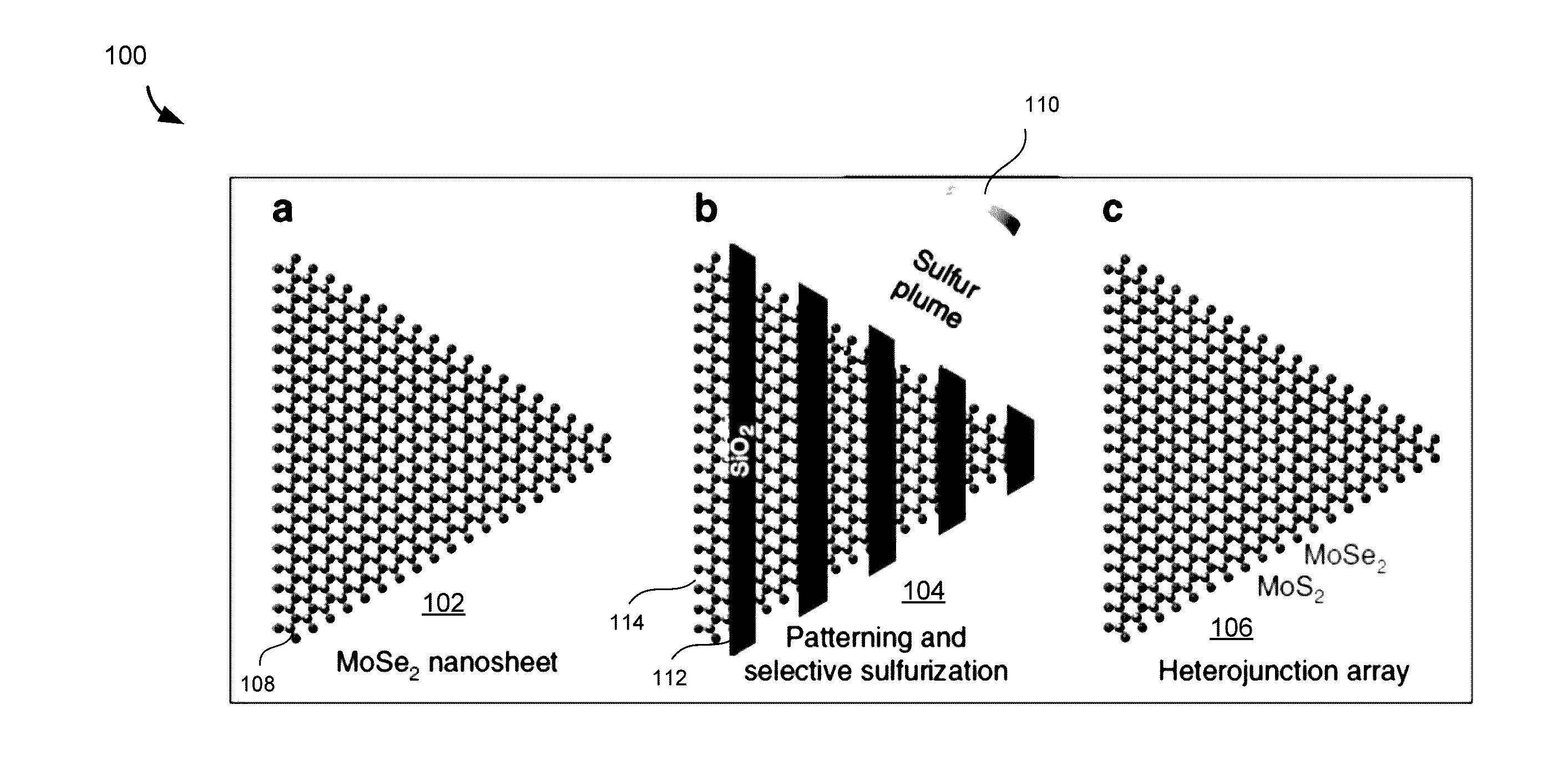
[0028]High density integration of semiconductor heterojunctions forms the foundation of modern electronics and optoelectronics. Methods for deterministically producing lateral heterojunctions in two-dimensional crystal nanostructures may lead the way in the advancement of next-generation electronics.

[0029]Lateral heterojunctions may be synthesized in lithographically patterned arrays over a two-dimensional nanostructure crystal by selectively converting exposed regions of the nanostructure crystal from a first composition of matter into a different composition of matter. The amount of matter converted, or doping level, within the exposed regions may be varied with precision. The host nanostructure crystal, before and after the conversion process, may comprise a two dimensional monolayer or few-layer crystal, such as bilayer or trilayer lattice structure, all of which may be referred to as a nanosheet or nanostructure.

[0030]The shapes and stoichiometry of designed patterned regions a...


PUM


Abstract

Methods, articles of manufacture and systems for creating new nanoscale two dimensional materials comprising designed arrays of lateral or vertical heterojunctions may be fabricated by first lithographically masking a 2D material. Exposed, or unmasked, regions of the 2D material may be converted to a different composition of matter to form lateral or vertical heterojunctions according to the patterned mask. PLD and high kinetic energy impingement of atoms may replace or add atoms in the exposed regions, and a plurality of the exposed regions may be converted concurrently. The process may be repeated one or more times on either side of the same 2D material to form any suitable combination of lateral heterojunctions and/or vertical heterojunctions, comprising semiconductors, metals or insulators or any suitable combination thereof. Furthermore, the resulting 2D material may comprise p-n, n-n, p-p, n-p-n and p-n-p junctions, or any suitable combination thereof.

Description

CROSS REFERENCES TO RELATED APPLICATIONS[0001]This patent application makes reference to and claims priority to U.S. Provisional Patent Application Ser. No. 62 / 195,150, filed on Jul. 21, 2015, which is hereby incorporated by reference in its entirety.STATEMENT REGARDING FEDERALLY FUNDED RESEARCH AND DEVELOPMENT[0002]The United States Government has rights in this invention pursuant to contract no. DE-AC05-00OR22725 between the United States Department of Energy and UT-Battelle, LLC.BACKGROUND OF THE INVENTION[0003]1. Technical Field[0004]This disclosure relates generally to two dimensional (2D) electronic materials. Specifically, the disclosure pertains to the synthesis and patterning of 2D materials in controlled configurations for devices.[0005]2. Related Art[0006]2D nanostructure materials are the latest in a long line of useful materials that hold great promise for high-density electronics. Because of their nanoscale dimensions, electrons become quantum confined within and imbue...

Claims


Application Information

Patent Timeline
IPC IPC(8): H01L29/267G03F1/20H01L21/027H01L21/033H01L21/02
CPCH01L29/267H01L21/0332H01L21/02164G03F1/20H01L21/02568H01L21/02609H01L21/0277H01L21/02664H01L29/735H01L29/778H01L29/0661H01L29/1606H01L29/24
Inventor GEOHEGAN, DAVID B.ROULEAU, CHRISTOPHER M.WANG, KAIXIAO, KAILIN, MING-WEIPURETZKY, ALEXANDER A.MAHJOURI-SAMANI, MASOUD
Owner UT BATTELLE LLC
Why Eureka
Try Eureka