Method of obtaining planar semipolar gallium nitride surfaces

a gallium nitride and surface technology, applied in the direction of basic electric elements, electrical equipment, semiconductor devices, etc., can solve the problems of iii-nitride materials that are typically more difficult and expensive to grow, bulk substrates of iii-nitride materials larger than a few inches in diameter are not currently commercially feasible, and achieve the effect of preventing nucleation and growth

Active Publication Date: 2017-02-02
YALE UNIV
View PDF1 Cites 16 Cited by
  • Summary
  • Abstract
  • Description
  • Claims
  • Application Information

AI Technical Summary

Benefits of technology

[0007]Methods and structures associated with forming planar semipolar gallium nitride (GaN) layers and other semipolar III-nitride layers on patterned sapphire substrates (PSS) is described. A sapphire substrate may be patterned with a surface-grating structure to expose c-plane or inclined c-plane surfaces, and semipolar III-nitride semiconductor may be grown from these crystal-growth surfaces. A masking process may be carried out prior to semiconductor growth to prevent nucleation and growth at other surfaces of the patterned sapphire substrate. Growth of the semipolar material may be continued, so that the material coalesces and forms a continuous III-nitride layer over the patterned sapphire substrate. The semiconductor layer may be planarized and III-nitride material regrown over the planarized layer. During regrowth, a nitrogen carrier gas, instead of a hydrogen carrier gas, may be used to provide a flat, semipolar, atomically-smooth process surface on which integrated devices may be fabricated.

Problems solved by technology

Unlike silicon, III-nitride materials are typically more difficult and expensive to grow than silicon, so that bulk substrates of III-nitride materials larger than a few inches in diameter are not currently as commercially feasible as bulk silicon substrates.

Method used


Image

  • Method of obtaining planar semipolar gallium nitride surfaces
  • Method of obtaining planar semipolar gallium nitride surfaces
  • Method of obtaining planar semipolar gallium nitride surfaces

Examples


examples

1. Formation of Planar, Semipolar GaN Epilayers

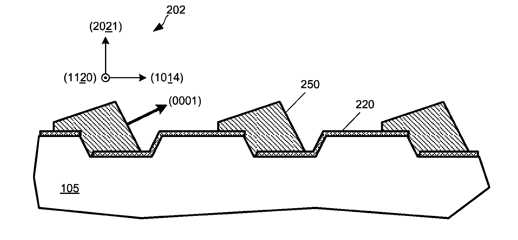
[0072]Epitaxial growth, planarization, and regrowth of semipolar (2021) GaN was carried out on patterned sapphire substrates following the methods described above. In these example processes, the sapphire substrates had a diameter of 2 inches, though other diameters may be used following the same processes.

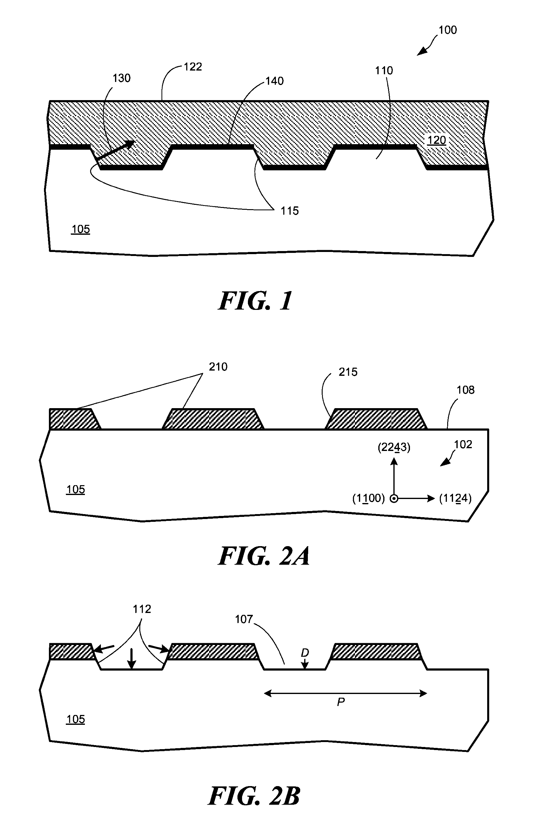
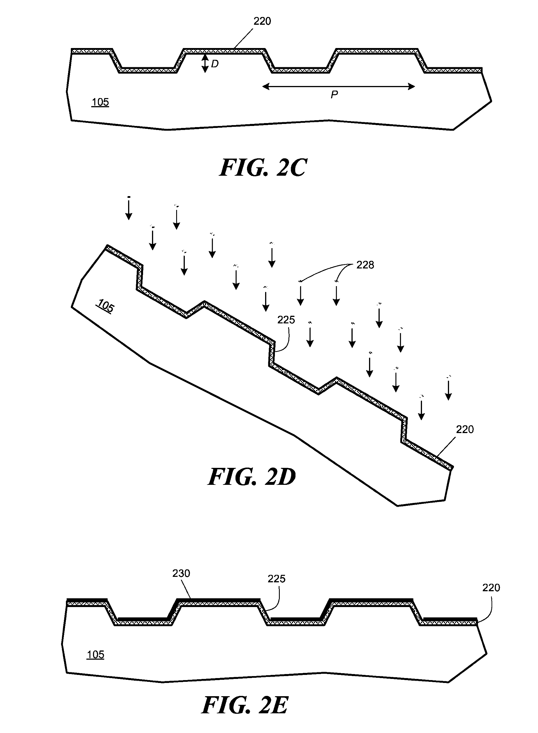
[0073]A sapphire substrate having a (2243) facet parallel to its surface was patterned following the steps described in connection with FIGS. 2A-2B and comprised crystal-growth surfaces 115 spaced approximately 6 μm apart, and the etch depth D of trenches in the sapphire substrate is approximately 0.5 μm. The crystal-growth surfaces were oriented at approximately 75° from the process surface of the substrate. Other surfaces on the PSS substrate were masked with a PECVD oxide, as described above in connection with FIGS. 2C-2F.

[0074]After cleaning, the PSS was loaded into a MOCVD reactor for III-nitride growth. A thermal cleaning and de...


PUM

PropertyMeasurementUnit
temperatureaaaaaaaaaa
pressureaaaaaaaaaa

Abstract

Methods and structures for forming flat, continuous, planar, epitaxial layers of semipolar III-nitride materials on patterned sapphire substrates are described. Semipolar GaN may be grown from inclined c-plane facets on a patterned sapphire substrate, and coalesced to form a continuous layer of semipolar III-nitride semiconductor over the sapphire substrate. Planarization of the layer is followed by crystal regrowth using a nitrogen carrier gas to produce a flat, microfabrication-grade, process surface of semipolar III-nitride semiconductor across the substrate. Quality multiple quantum wells can be fabricated in the regrown semipolar material.

Description

RELATED APPLICATIONS[0001]This application claims the benefit of U.S. provisional Application Ser. No. 61 / 980,304, titled “Method of Obtaining Planar Semipolar Gallium Nitride Surfaces,” filed on Apr. 16, 2014. The entire disclosure of the foregoing application is incorporated herein by reference.BACKGROUND[0002]1. Technical Field[0003]The technology relates to methods and structures for forming planar, single-facet semipolar III-nitride layers and devices on patterned sapphire substrates.[0004]2. Discussion of the Related Art[0005]Gallium nitride (GaN) and other III-nitride materials are widely recognized as desirable materials for fabrication of integrated devices. These materials typically have wider band gaps than silicon-based semiconductors and can be used to make electro-optical devices (e.g., LEDs and diode lasers) that emit radiation in the green and blue regions of the visible spectrum. Also, because of their wide band-gap, III-nitride materials can exhibit higher breakdow...

Claims


Application Information

Patent Timeline
Patent Type & Authority Applications(United States)
IPC IPC(8): H01L29/20H01L21/306H01L29/15H01L21/02
CPCH01L29/2003H01L21/0242H01L21/0243H01L21/02433H01L21/0254H01L29/15H01L21/0262H01L21/02458H01L21/02639H01L21/02647H01L21/30625H01L21/02609H01L29/045H01L29/155
Inventor HAN, JUNGLEUNG, BENJAMIN
Owner YALE UNIV
Why Eureka
Try Eureka