LED package, backlight unit and illumination device including same, and liquid crystal display including backlight unit

a technology of backlight unit and illumination device, which is applied in the direction of identification means, lighting and heating apparatus, instruments, etc., can solve the problems of deterioration of color purity and lack of uniform luminance, and achieve the effects of improving color reproducibility and color purity, preventing the deterioration of semiconductor nanocrystals, and high reliability

Active Publication Date: 2017-03-23
SAMSUNG ELECTRONICS CO LTD
View PDF12 Cites 29 Cited by
  • Summary
  • Abstract
  • Description
  • Claims
  • Application Information

AI Technical Summary

Benefits of technology

[0009]In one embodiment, an LED (light emitting diode) package is provided having a structure being capable of uniformly dispersing the light emitted from the LED light source, having improved color reproducibility and color purity and having high reliability as it is able to prevent the deterioration of semiconductor nanocrystal.

Problems solved by technology

However, the use of the CCFL as a light source may result in a lack of uniform luminance and may demonstrate deteriorated color purity when the LCD device has a larger screen.

Method used


Image

  • LED package, backlight unit and illumination device including same, and liquid crystal display including backlight unit
  • LED package, backlight unit and illumination device including same, and liquid crystal display including backlight unit
  • LED package, backlight unit and illumination device including same, and liquid crystal display including backlight unit

Examples


example 1

Manufacture of LED Package

[0297]InZnP / ZnSeS / ZnS green semiconductor nanocrystals with a light emitting wavelength of 531 nm are dispersed into 421.8 milliliter (mL) of toluene to have an optical density (OD) (absorbance at a first absorption maximum wavelength in the UV-Vis absorption spectrum of a 100-fold diluted solution) of 0.069, to prepare a green semiconductor nanocrystal dispersion liquid.

[0298]InP / ZnSeS / ZnS red semiconductor nanocrystals having a light emitting wavelength of 619 nm, are dispersed into 111.4 mL of toluene to have an optical density (OD) (absorbance at a first absorption maximum wavelength in the UV-Vis absorption spectrum of a 100-fold diluted solution) of 0.028, to prepare a red semiconductor nanocrystal dispersion liquid.

[0299]The green semiconductor nanocrystal dispersion liquid and the red semiconductor nanocrystal dispersion liquid are mixed, and the resultant is mixed with 100 mL of ethanol followed by centrifugation. The supernatant of the solution ex...

example 2

Manufacture of LED Package

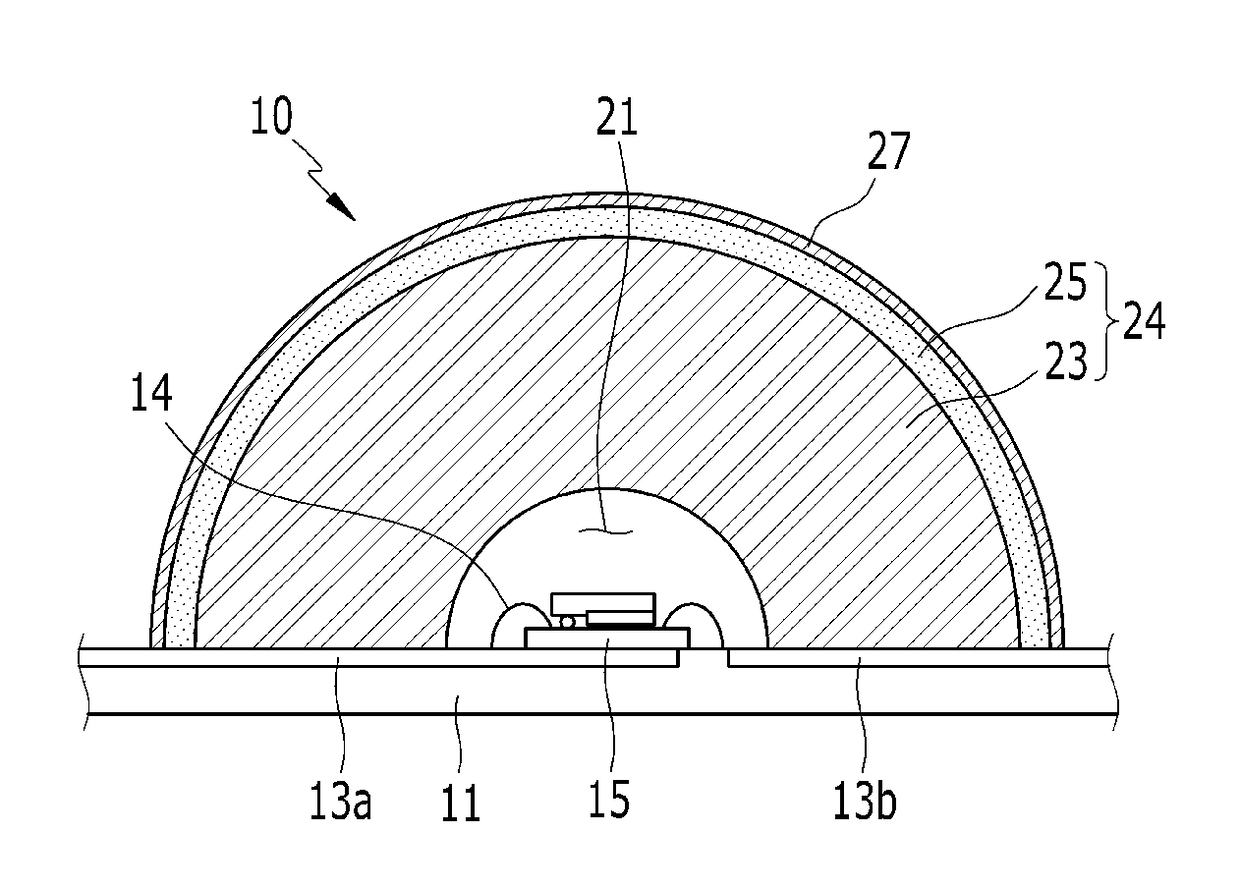
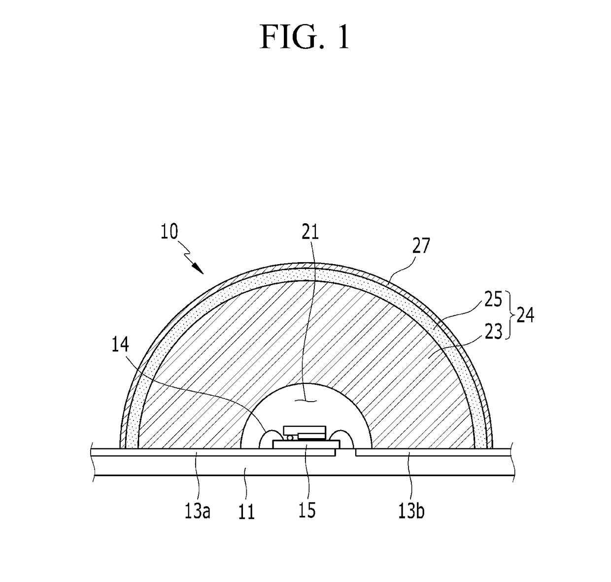
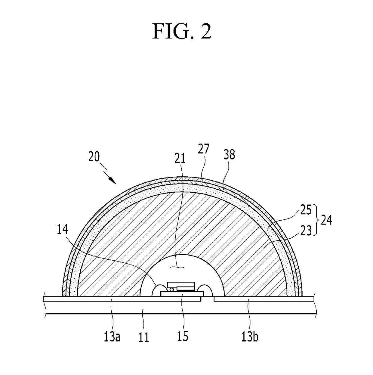
[0303]An LED package having a structure shown in FIG. 3 is fabricated in accordance with the same procedure as in Example 1, except that a second inorganic barrier layer of a silica layer is additionally formed between the light-scattering structure and the light conversion layer according to Example 1.


PUM

PropertyMeasurementUnit
transmittanceaaaaaaaaaa
glass transition temperatureaaaaaaaaaa
refractive indexaaaaaaaaaa

Abstract

A light emitting diode (LED) package includes: an LED; a stack structure including a light-scattering structure spaced apart from the LED, and a light conversion layer disposed on at least one surface selected from an inner surface and an outer surface of the light-scattering structure and configured to convert light emitted from the LED into white light, wherein the light conversion layer includes a semiconductor nanocrystal; and an organic barrier layer disposed on a surface of the light conversion layer.

Description

CROSS REFERENCE TO RELATED APPLICATIONS[0001]This application claims priority to and the benefit of Korean Patent Application Nos. 10-2015-0134213 and 10-2016-0120986, filed in the Korean Intellectual Property Office on Sep. 22, 2015 and Sep. 21, 2016, respectively and all the benefits accruing therefrom under 35 U.S.C. §119, the content of which in its entirety is incorporated herein by reference.BACKGROUND[0002]1. Field[0003]A light emitting diode (LED) package, and a backlight unit, and an illumination device including the same are disclosed. A liquid crystal display device including the backlight unit is also disclosed.[0004]2. Description of the Related Art[0005]Liquid crystal display (“LCD”) devices form an image by receiving external light, unlike plasma display panels (“PDPs”) and field emission displays (“FEDs”) which form an image using self-emitting light. Thus, the LCD device includes a backlight unit on the rear side thereof for emitting light.[0006]As a type of backlig...

Claims


Application Information

Patent Timeline
Patent Type & Authority Applications(United States)
IPC IPC(8): G02F1/1335H01L33/50C09D133/02C09K11/70C09K11/88C09K11/56H01L33/58H01L33/56H05B44/00
CPCG02F1/133603H01L33/58H01L33/502H01L33/501H01L33/56G02F1/133609G02F2202/08C09K11/70C09K11/883C09K11/565C09D133/02G02F2001/133614G02F2202/36G02F1/133606H01L2224/16145H01L2224/48091H01L33/507H01L2933/0091Y02B20/00G02F1/133614G02F1/133607H05B45/00H01L2924/00014H01L2924/12041G09F9/33F21Y2115/10G02B6/0073G09F2013/222H05K2201/10106G02B19/0066
Inventor JANG, EUN JOOKANG, HYUN AJUN, SHIN AECHO, OUL
Owner SAMSUNG ELECTRONICS CO LTD
Why Eureka
Try Eureka