Imaging device, module, electronic device, and method of operating the imaging device

a technology of imaging device and charge retention portion, which is applied in the direction of radio frequency controlled devices, transistors, television systems, etc., can solve the problems of difficult circuit structure and long time-consuming, and achieve the effect of low noise, high resolution and high-integration imaging devices

Active Publication Date: 2017-03-23
SEMICON ENERGY LAB CO LTD
View PDF11 Cites 17 Cited by
  • Summary
  • Abstract
  • Description
  • Claims
  • Application Information

AI Technical Summary

Benefits of technology

[0012]In the case where the pixel area is reduced, it is also effective to reduce not only a design rule but also the number of devices such as transistors. For example, some transistors included in a pixel circuit are used in common by a plurality of pixels.
[0014]An object of one embodiment of the present invention is to provide an imaging device where a transistor can be used in common by a plurality of pixels. Another object of one embodiment of the present invention is to provide an imaging device where a wiring can be used in common by a plurality of pixels. Another object of one embodiment of the present invention is to provide an imaging device that has a structure where a transistor is used in common by a plurality of pixels and that is capable of imaging with a global shutter system. Another object of one embodiment of the present invention is to provide an imaging device that reads, in an exposure period, data of an image taken in the previous frame. Another object of one embodiment of the present invention is to provide an imaging device capable of imaging with little noise. Another object of one embodiment of the present invention is to provide an imaging device that is suitable for high-speed operation. Another object of one embodiment of the present invention is to provide an imaging device with high resolution. Another object of one embodiment of the present invention is to provide a highly integrated imaging device. An object of one embodiment of the present invention is to provide an imaging device capable of imaging under a low illuminance condition. Another object of one embodiment of the present invention is to provide an imaging device that can be used in a wide temperature range. Another object of one embodiment of the present invention is to provide an imaging device with a high aperture ratio. Another object of one embodiment of the present invention is to provide an imaging device with high reliability. Another object of one embodiment of the present invention is to provide a novel imaging device or the like. Another object of one embodiment of the present invention is to provide a method for driving any of the imaging devices. Another object of one embodiment of the present invention is to provide a novel semiconductor device or the like.
[0025]According to one embodiment of the present invention, an imaging device where a transistor can be used in common by a plurality of pixels can be provided. An imaging device where a wiring can be used in common by a plurality of pixels can be provided. An imaging device that has a structure where a transistor is used in common by a plurality of pixels and that is capable of imaging with a global shutter system can be provided. An imaging device that reads, in an exposure period, data of an image taken in the previous frame can be provided. An imaging device capable of imaging with little noise can be provided. An imaging device that is suitable for high-speed operation can be provided. An imaging device with high resolution can be provided. A highly integrated imaging device can be provided. An imaging device capable of imaging under a low illuminance condition can be provided. An imaging device that can be used in a wide temperature range can be provided. An imaging device with a high aperture ratio can be provided. An imaging device with high reliability can be provided. A novel imaging device or the like can be provided. A method for operating any of the imaging devices can be provided. A novel semiconductor device or the like can be provided.

Problems solved by technology

However, in the global shutter system, imaging data are obtained in all the pixels at the same time and sequentially read; thus, the data need to be retained in a charge retention portion for a long time.
Therefore, when operation with the global shutter system is assumed, it is difficult to employ a circuit structure where a charge retention portion or the like is used in common by a plurality of pixels.

Method used


Image

  • Imaging device, module, electronic device, and method of operating the imaging device
  • Imaging device, module, electronic device, and method of operating the imaging device
  • Imaging device, module, electronic device, and method of operating the imaging device

Examples


embodiment 1

[0100]In this embodiment, an imaging device that is one embodiment of the present invention is described with reference to drawings.

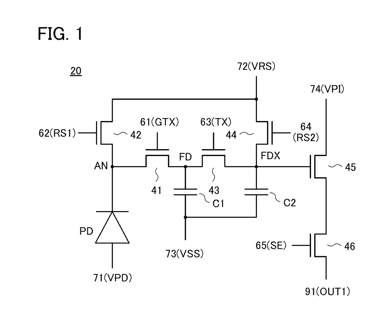
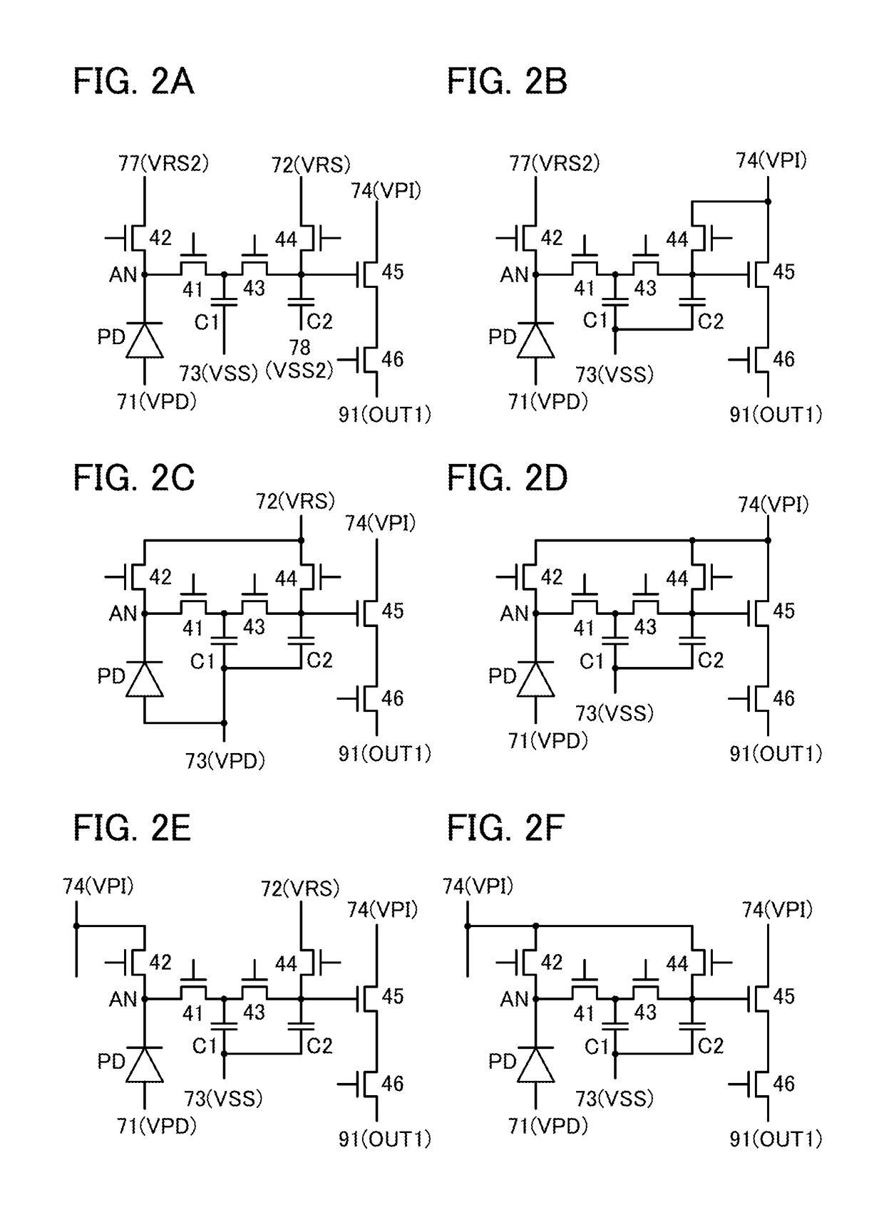
[0101]One embodiment of the present invention relates to an imaging device that has a circuit structure where a transistor that resets the potential of a charge detection portion, a transistor that outputs a signal corresponding to the potential of the charge detection portion, and a transistor that selects a pixel are used in common by a plurality of pixels and that is capable of imaging with a global shutter system, and a method for driving the imaging device. In the imaging device, imaging data can be obtained in an n-th frame (n is a natural number of 1 or more) and the imaging data can be read in an (n+1)th frame.

[0102]The number of transistors per pixel can be reduced, so that the pixel area can be reduced. In other words, pixels can be highly integrated. Since the imaging data is read in the (n+1)th frame, imaging time in the n-th frame can be ma...

embodiment 2

[0240]In this embodiment, a transistor including an oxide semiconductor that can be used in one embodiment of the present invention is described with reference to drawings. In the drawings in this embodiment, some components are enlarged, reduced in size, or omitted for easy understanding.

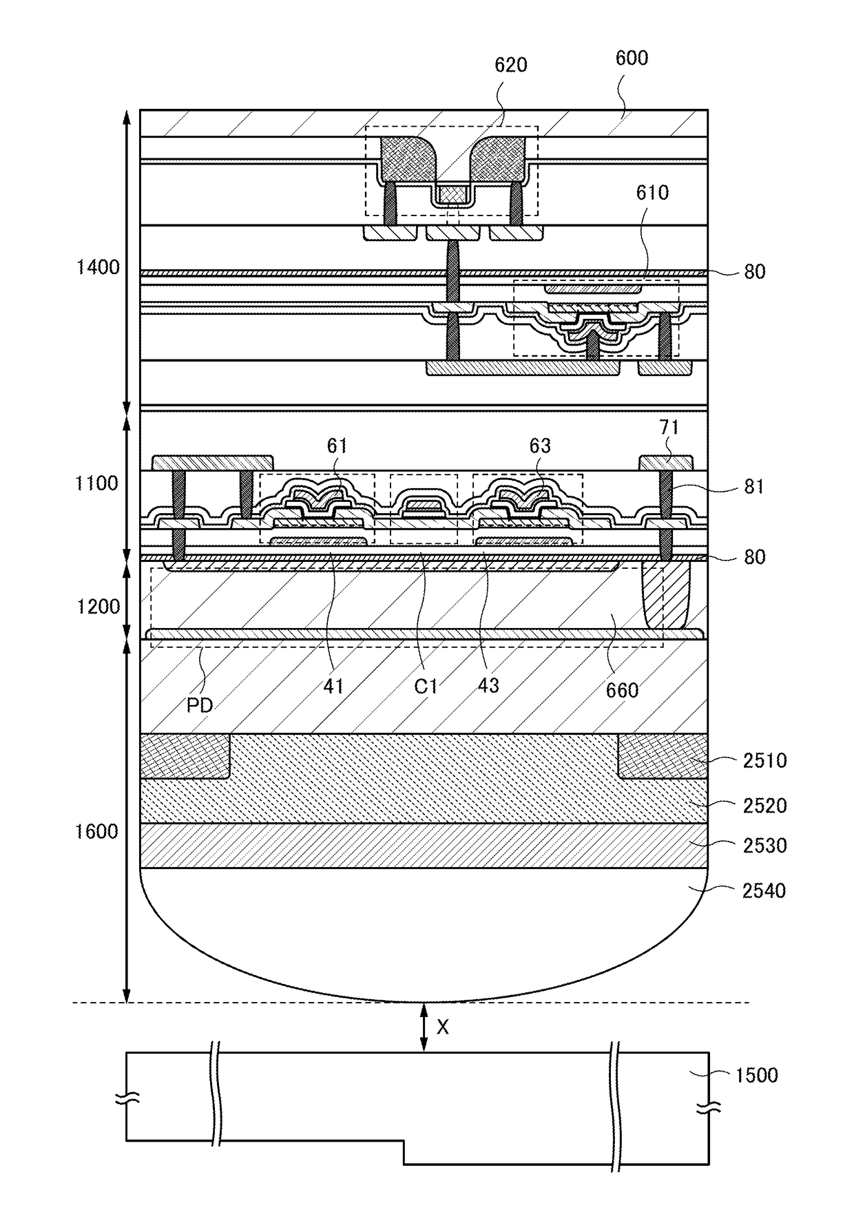
[0241]FIGS. 36A and 36B are a top view and a cross-sectional view illustrating a transistor 101 in one embodiment of the present invention. FIG. 36A is a top view, and a cross section in the direction of dashed-dotted line B1-B2 in FIG. 36A is illustrated in FIG. 36B. A cross section in the direction of dashed-dotted line B3-B4 in FIG. 36A is illustrated in FIG. 38A. The direction of dashed-dotted line B1-B2 is referred to as a channel length direction, and the direction of dashed-dotted line B3-B4 is referred to as a channel width direction.

[0242]The transistor 101 includes an insulating layer 120 in contact with a substrate 115; an oxide semiconductor layer 130 in contact with the insulating laye...

embodiment 3

[0305]In this embodiment, components of the transistors described in Embodiment 2 are described in detail.

[0306]As the substrate 115, a glass substrate, a quartz substrate, a semiconductor substrate, a ceramic substrate, a metal substrate having a surface subjected to insulation treatment, or the like can be used. The substrate 115 can be a silicon substrate provided with a transistor and / or a photodiode; and an insulating layer, a wiring, a conductor functioning as a contact plug, and the like that are provided over the silicon substrate. Note that when p-channel transistors are formed using the silicon substrate, a silicon substrate with n−-type conductivity is preferably used. Alternatively, an SOI substrate including an n−-type or i-type silicon layer may be used. In the case where a p-channel transistor is formed using the silicon substrate, a surface of the silicon substrate where the transistor is formed preferably has a (110) plane orientation. Forming a p-channel transistor...


PUM


Abstract

An imaging device that has a structure where a transistor is used in common by a plurality of pixels and is capable of imaging with a global shutter system is provided. A transistor that resets the potential of a charge detection portion, a transistor that outputs a signal corresponding to the potential of the charge detection portion, and a transistor that selects a pixel are used in common by the plurality of pixels. A node AN (a first charge retention portion), a node FD (a second charge retention portion), and a node FDX (the charge detection portion) are provided. Imaging data obtained in the node AN is transferred to the node FD, and the imaging data is sequentially transferred from the node FD to the node FDX to be read.

Description

BACKGROUND OF THE INVENTION[0001]1. Field of the Invention[0002]One embodiment of the present invention relates to an imaging device and an operation method thereof.[0003]Note that one embodiment of the present invention is not limited to the above technical field. The technical field of one embodiment of the invention disclosed in this specification and the like relates to an object, a method, or a manufacturing method. One embodiment of the present invention relates to a process, a machine, manufacture, or a composition of matter. Specifically, examples of the technical field of one embodiment of the present invention disclosed in this specification include a semiconductor device, a display device, a liquid crystal display device, a light-emitting device, a lighting device, a power storage device, a storage device, an imaging device, a method for operating any of them, and a method for manufacturing any of them.[0004]In this specification and the like, a semiconductor device gener...

Claims


Application Information

Patent Timeline
Patent Type & Authority Applications(United States)
IPC IPC(8): H01L27/146H04N5/225H04N5/378H01L31/0272
CPCH01L27/14616H01L31/0272H01L27/14627H04N5/2253H01L27/14645H04N5/2254H04N5/378H01L27/14603H01L27/14612H04N23/50H04N25/62H04N25/77H04N25/75H04N5/32H04N23/54H04N25/531H04N25/778H04N25/771H01L27/1203H01L27/14665H01L27/1225H01L27/14643H04N25/772
Inventor OHMARU, TAKUROKUSUMOTO, NAOTO
Owner SEMICON ENERGY LAB CO LTD
Why Eureka
Try Eureka