Semiconductor device

a technology of semiconductor devices and semiconductors, applied in semiconductor devices, semiconductor/solid-state device details, electrical apparatus, etc., can solve the problems of reducing the contact area between the heat sink and the package, and achieve the effect of reducing the stress on the package, and increasing the distance between the recess portions

Inactive Publication Date: 2017-03-30
DENSO CORP
View PDF8 Cites 12 Cited by
  • Summary
  • Abstract
  • Description
  • Claims
  • Application Information

AI Technical Summary

Benefits of technology

[0007]During operation of the semiconductor device, the semiconductor elements generate heat, and the heat sinks thereby thermally expand and the package also thermally expands. Because of a difference in thermal expansion coefficient between the heat sinks and the package, stress acts on both the heat sink and the package. In such cases, as in JP 2014-154779 A, formation of recess portions in an outer peripheral end face of a molded resin causes the stress to be concentrated on the recess portions. In order to reduce stress on a package, a structure in which heat sinks are downsized may be employed. This structure enables increase of a distance between recess portions and the heat sinks, and thus enables reduction of stress on the recess portions. However, the downsizing of the heat sinks results in decrease in area of contact between the heat sinks and the package. The present disclosure provides a technique that reduces stress imposed on recess portions during operation of a semiconductor device while maintaining semiconductor element protection performance.

Problems solved by technology

However, the downsizing of the heat sinks results in decrease in area of contact between the heat sinks and the package.

Method used


Image

  • Semiconductor device
  • Semiconductor device
  • Semiconductor device

Examples


embodiment 1

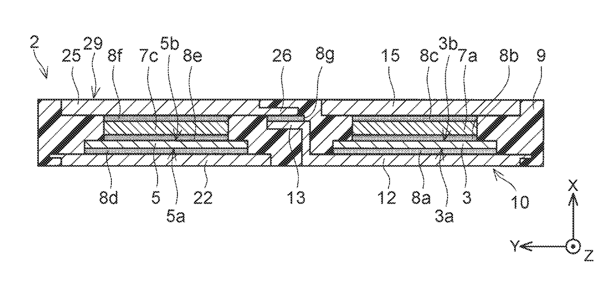
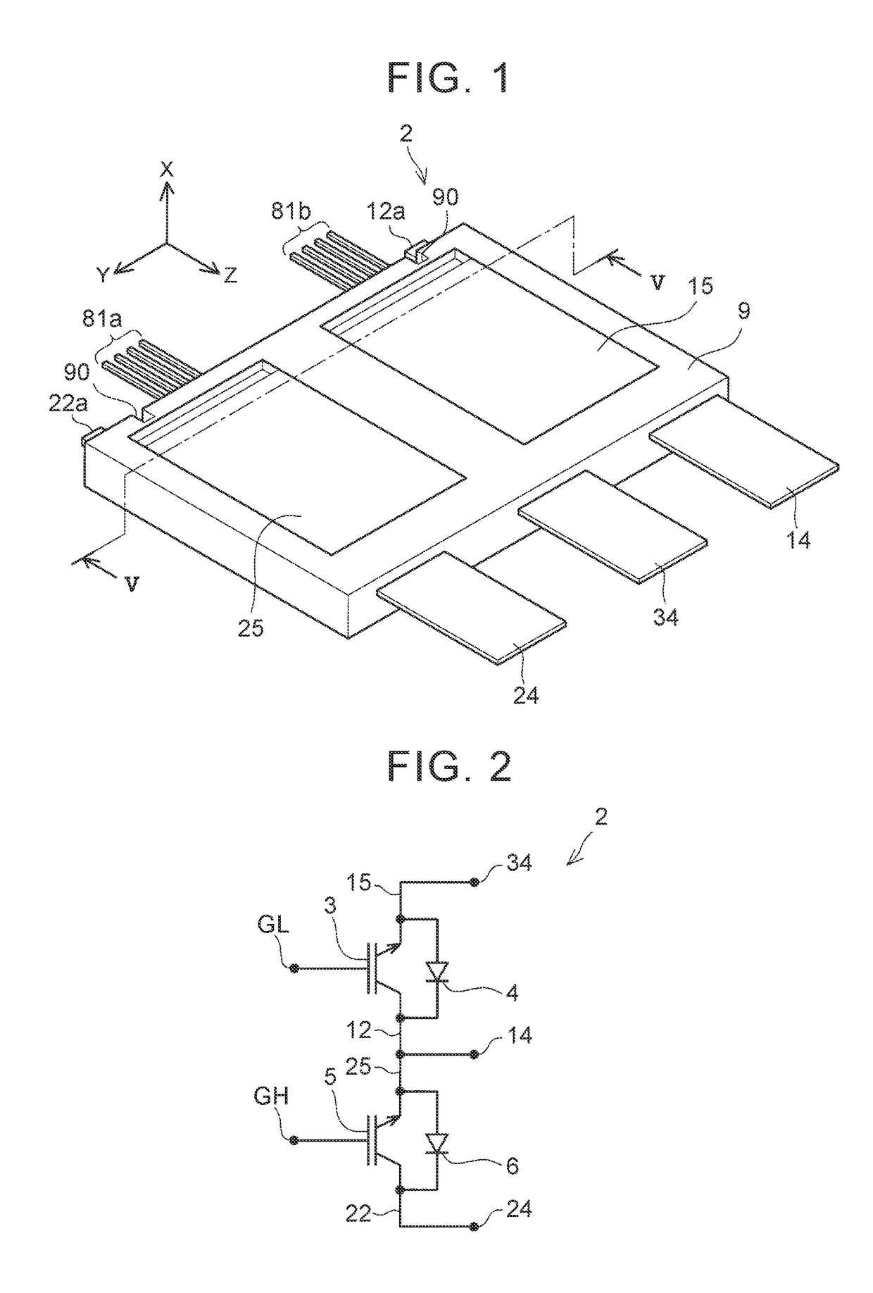
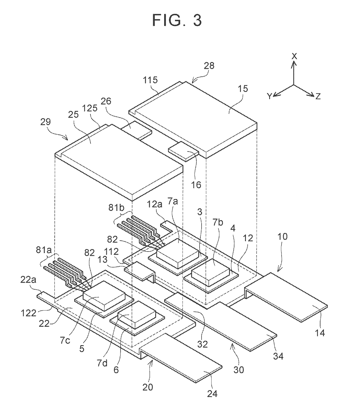
[0029]A semiconductor device 2 will be described with reference to the drawings. FIG. 2 is a diagram of a circuit incorporated in the semiconductor device 2. The semiconductor device 2 includes a first transistor element 3, a second transistor element 5, a first diode element 4, a second diode element 6, an N terminal 34, an O terminal 14 and a P terminal 24. Each of the first transistor element 3, the second transistor element 5, the first diode element 4 and the second diode element 6 has an ampacity of 100 amperes or more, and belongs to a power semiconductor element mainly used for electric power conversion. The semiconductor device 2 typically forms a part of an inverter circuit that supplies electric power to a drive motor in, e.g., an electric vehicle, a hybrid vehicle or a fuel cell vehicle.

[0030]The first transistor element 3 and the second transistor element 5 are connected in series. The first diode element 4 is connected in inverse parallel with the first transistor ele...

embodiment 2

[0049]As illustrated in FIG. 8, in the semiconductor device , each of thin portions 112, 115 of heat sinks 12, 15 are covered by a package 9. Each thin portion is sealed by the package 9 and is not exposed outside. Although not illustrated, thin portions 122, 125 of heat sinks 22, 25 each have a configuration similar to that of the heat sinks 12, 15. This configuration enables increase in area of contact between the heat sinks and the package 9, and thus enables further enhancement in power semiconductor element protection performance.

[0050]As illustrated in FIG. 9, in a semiconductor device according to Embodiment 3, thin portions 112, 115 are formed by reducing a thickness of respective parts on the inner face side of the heat sink 12, 15. The thin portions 112, 115 are formed by dents that are present in the inner faces of the heat sinks 12, 15, and the dents are sealed by the package 9. Although not illustrated, thin portion 122, 125 of heat sinks 22, 25 have a configuration sim...

embodiment 4

[0051]As illustrated in FIG. 10, in a semiconductor device , thin portions 115, 125 are formed by cutting a plurality of parts (in the present embodiment, three parts along the Y-axis direction on the periphery of an end portion in the negative direction of the Z axis) in an outer face of each of heat sinks 15, 25 into a cylindrical shape. The thin portions 115, 125 do not extend through the respective heat sinks vertically. Although not illustrated, thin portions 112, 122 of heat sinks 12, 22 have a configuration similar to that of the heat sinks 15, 25. Also, each of the thin portions 112, 122 is also located on a shortest distance between a relevant power semiconductor element and a relevant recess portion. This configuration causes stress generated by thermal expansion of the heat sinks to be dispersed toward the inside of the thin portions, enabling reduction of concentration of stress on the recess portions 90.


PUM


Abstract

A semiconductor device includes: a semiconductor element; a heat sink including a first surface and a second surface, the semiconductor element being joined to the first surface, the second surface being a surface on an opposite side of the first surface; and a package that is in contact with the semiconductor element and the first surface of the heat sink, the package including a recess portion in an outer face, wherein the heat sink includes a thick portion, and a thin portion having a thickness that is smaller than that of the thick portion, and the thin portion is located on a line connecting an outer face of the semiconductor element and the recess portion in a shortest distance.

Description

CROSS-REFERENCE TO RELATED APPLICATIONS[0001]The present disclosure claims priority to Japanese Patent Application No. 2015-188240 filed on Sep. 25, 2015, which is incorporated herein by reference in its entirety including the specification, drawings and abstract.BACKGROUND[0002]1. Field of the Disclosure[0003]The present disclosure relates to a semiconductor device.[0004]2. Description of Related Art[0005]Japanese Patent Application Publication No. 2014-154779 discloses a semiconductor device including semiconductor elements fixed to heat sinks, a periphery of the semiconductor elements being sealed by resin molding. Each semiconductor element includes an outer peripheral end face, and each heat sink includes an inner face, an outer face and an outer peripheral end face. The semiconductor elements are fixed to inner faces of the respective heat sinks, and the respective outer peripheral end faces of the semiconductor elements fixed to the heat sinks are exposed. The molded resin co...

Claims


Application Information

Patent Timeline
Patent Type & Authority Applications(United States)
IPC IPC(8): H01L23/367H01L23/00H01L25/18H01L23/31
CPCH01L23/3675H01L23/3142H01L24/33H01L2924/13055H01L2224/32245H01L2224/33181H01L2924/1203H01L25/18H01L23/3185H01L23/3672H01L23/562H01L23/3735H01L23/4334H01L24/06H01L24/29H01L24/32H01L24/48H01L24/73H01L2224/04026H01L2224/04042H01L2224/06181H01L2224/291H01L2224/48247H01L2224/73215H01L2224/73265H01L2924/1815H01L23/051H01L23/3107H01L2924/00014H01L2924/181H01L2924/014H01L2924/00012H01L2224/45099
Inventor IWASAKI, SHINGOOKUMURA, TOMOMI
Owner DENSO CORP
Why Eureka
Try Eureka