Time sampled photodetector devices and methods

a photodetector and time-sampled technology, applied in the field of optical time-sampled photodetectors, can solve the problem of challenging the provision of suitable tias at such a wide rang

Active Publication Date: 2017-03-30
TRANSFERT PLUS S E C +1
View PDF9 Cites 7 Cited by
  • Summary
  • Abstract
  • Description
  • Claims
  • Application Information

AI Technical Summary

Problems solved by technology

However, an important consideration is the bandwidth mismatch between the optical PD and the electronic TIA circuit.
For example, whilst the bandwidth of a SiGe PD can be extended up to 60 GHz through exploiting inductive gain the provisioning of suitable TIAs at such bandwidth remains challenging.

Method used


Image

  • Time sampled photodetector devices and methods
  • Time sampled photodetector devices and methods
  • Time sampled photodetector devices and methods

Examples


Embodiment Construction

[0041]The present invention is directed to optical photodetectors and more particularly to optical time sampled photodetectors.

[0042]The ensuing description provides representative embodiment(s) only, and is not intended to limit the scope, applicability or configuration of the disclosure. Rather, the ensuing description of the embodiment(s) will provide those skilled in the art with an enabling description for implementing an embodiment or embodiments of the invention. It being understood that various changes can be made in the function and arrangement of elements without departing from the spirit and scope as set forth in the appended claims. Accordingly, an embodiment is an example or implementation of the inventions and not the sole implementation. Various appearances of “one embodiment,”“an embodiment” or“some embodiments” do not necessarily all refer to the same embodiments. Although various features of the invention may be described in the context of a single embodiment, the ...


PUM


Abstract

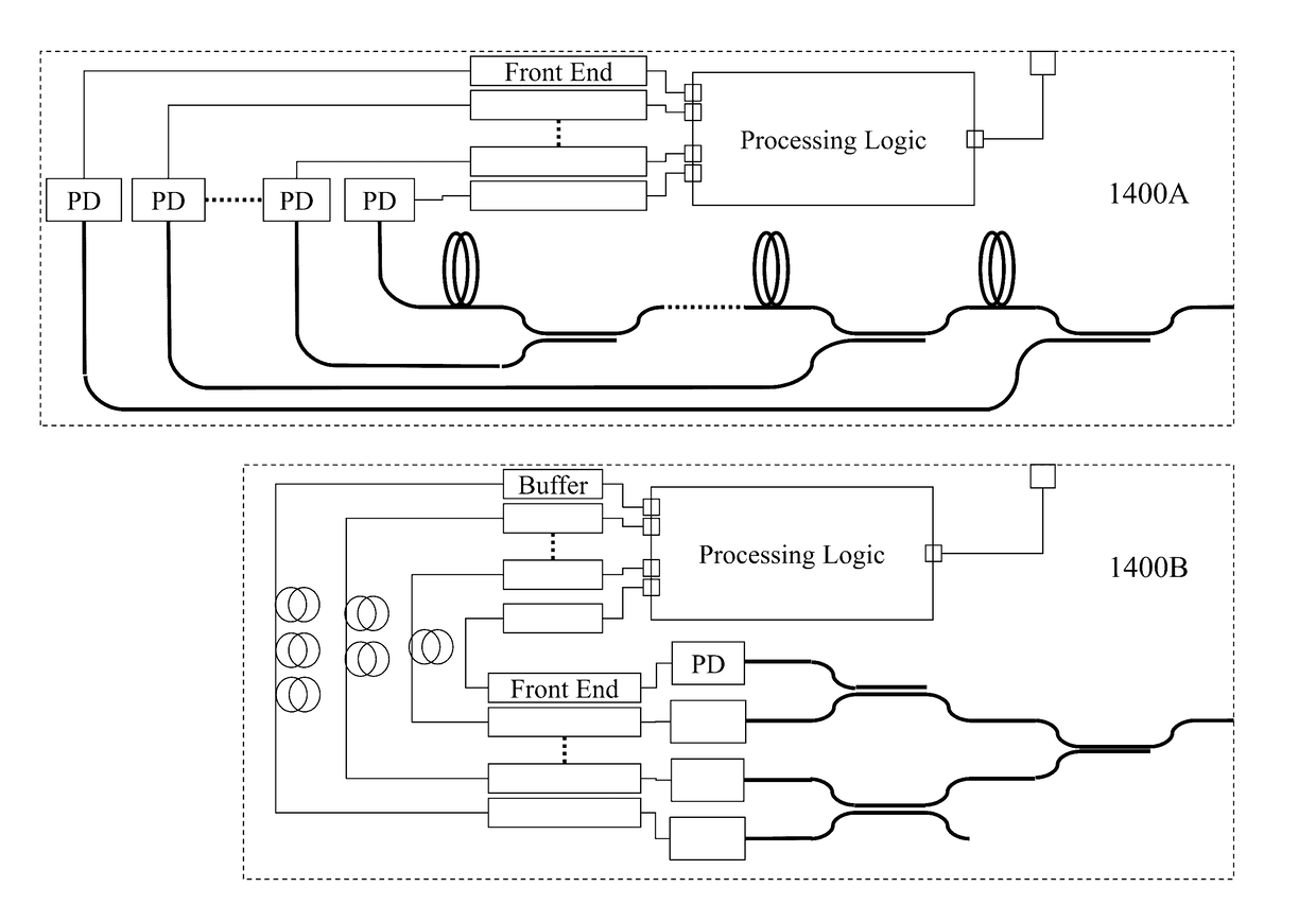
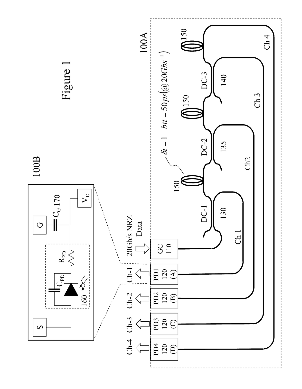
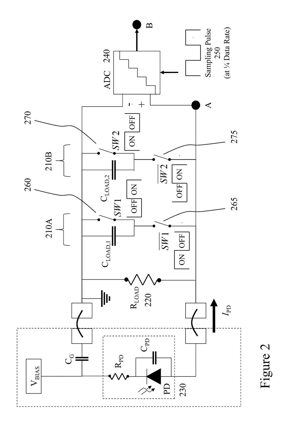
Photonic integration has primarily sought to exploit optical parallelism through wavelength division multiplexing whilst in many instances “brute-force” time division multiplexing offers benefits through reduced complexity and cost. However, photoreceivers are primarily the same now for operation at 10 Gb / s, 20 Gb / s, 40 Gb / s and above as 20 or 25 years ago and exploit the same optical detection—amplification—logic processing design. However, high speed low cost electronics ca be leveraged in conjunction with optical time sampling and logic to provide a new design paradigm. An incoming XGbs−1 optical data stream is sampled and processed by N photodetectors each operating at (X / N)Gbs−1 rather than the current direct XGbs−1 front-end of the prior art. Flexibility for the designer in establishing N within optical layer constraints, electronics capabilities etc. allows for further cost—power—complexity—performance tradeoffs to be established in different systems such that high capacity TDM links can exploit direct CMOS integrated optoelectronic front-ends.

Description

CROSS-REFERENCE TO RELATED APPLICATIONS[0001]This patent application claims the benefit of priority from U.S. Provisional Patent Application 62 / 232,645 filed Sep. 25, 2015 entitled “High-Speed Silicon Photonic Photoreceivers based on Optical Time Sampling”, the entire contents of which are incorporated herein by reference.FIELD OF THE INVENTION[0002]This invention relates to optical photodetectors and more particularly to optical time sampled photodetectors.BACKGROUND OF THE INVENTION[0003]Internet comprises over 100 billion plus web pages on over 100 million websites being accessed by nearly 3 billion users conducting approximately 3 billion Google searches per day, sending approximately 150 billion emails per day. With statistics like these the data being uploaded and downloaded every second on the Internet is staggering even before considering the expected growth of high bandwidth video in mobile applications etc. In 2016 user traffic is expected to exceed 100 exabytes per month,...

Claims


Application Information

Patent Timeline
Patent Type & Authority Applications(United States)
IPC IPC(8): H04B10/60G01J1/44
CPCG01J1/44H04B10/60G01J1/46H04B10/66
Inventor LIBOIRON-LADOUCEUR, ODILEHAI, MD. SHAFIQULMENARD, MICHAEL
Owner TRANSFERT PLUS S E C
Why Eureka
Try Eureka