Circuit module and method for manufacturing the same

a technology of circuit modules and circuit boards, applied in the field of circuit modules, can solve the problems of difficult formation of half-cut grooves and board breakage, and achieve the effects of reducing manufacturing costs, increasing connection reliability between shield layers and ground, and reducing manufacturing costs

Inactive Publication Date: 2017-04-06
MURATA MFG CO LTD
View PDF4 Cites 5 Cited by
  • Summary
  • Abstract
  • Description
  • Claims
  • Application Information

AI Technical Summary

Benefits of technology

[0016]According to a preferred embodiment of the present invention, the conductive joining material is applied to the front-surface-side ground electrode. Therefore, when the collective board is half-cut, not only can the portions of the interlayer vias be exposed in the half-cut grooves, but a portion of the conductive joining material applied to the front-surface-side ground electrode is also exposed in the half-cut grooves. Therefore, when the conductive shield layer is formed at the front-surface side of the half-cut collective board, the shield layer is able to be electrically connected not only to the interlayer vias but also to the conductive joining material. As a result, the shield layer is able to be connected to the ground not only through the ground interlayer vias but also through the conductive joining material, and the connection reliability between the shield layer and the ground is higher than that in the case where the conductive joining material is not provided.
[0017]When the electronic components are mounted on the collective board, the conductive joining material is applied to the front-surface-side ground electrode in addition to positions corresponding to the electronic components at the front surface of the collective board. Thus, the conductive joining material may be used to join the electronic components to the collective board, and may also be fixed to the front-surface-side ground electrode. Accordingly, the conductive joining material is able to be applied to the front-surface-side ground electrode at the time when the electronic components are mounted on the board, and it is not necessary to perform an additional step for applying the conductive joining material. Therefore, the yield is as high as that in the case where the conductive joining material is not applied to the front-surface-side ground electrode. In addition, since the connection reliability between the shield layer and the ground is able to be increased by using the conductive joining material for mounting the electronic components, the manufacturing cost is lower than that in the case where a connecting component different from that for the electronic components, for example, is used.

Problems solved by technology

However, it tends to be difficult to form a half-cut groove having an exact depth depending on, for example, the processing accuracy.
When the board has a small thickness, there is a risk that the internal electrode will not be exposed in the half-cut groove if the half-cut groove is too shallow, and there is a risk that the board will break if the half-cut groove is too deep.

Method used


Image

  • Circuit module and method for manufacturing the same
  • Circuit module and method for manufacturing the same
  • Circuit module and method for manufacturing the same

Examples


Embodiment Construction

[0034]Circuit modules according to preferred embodiments of the present invention will be described in detail with reference to the drawings.

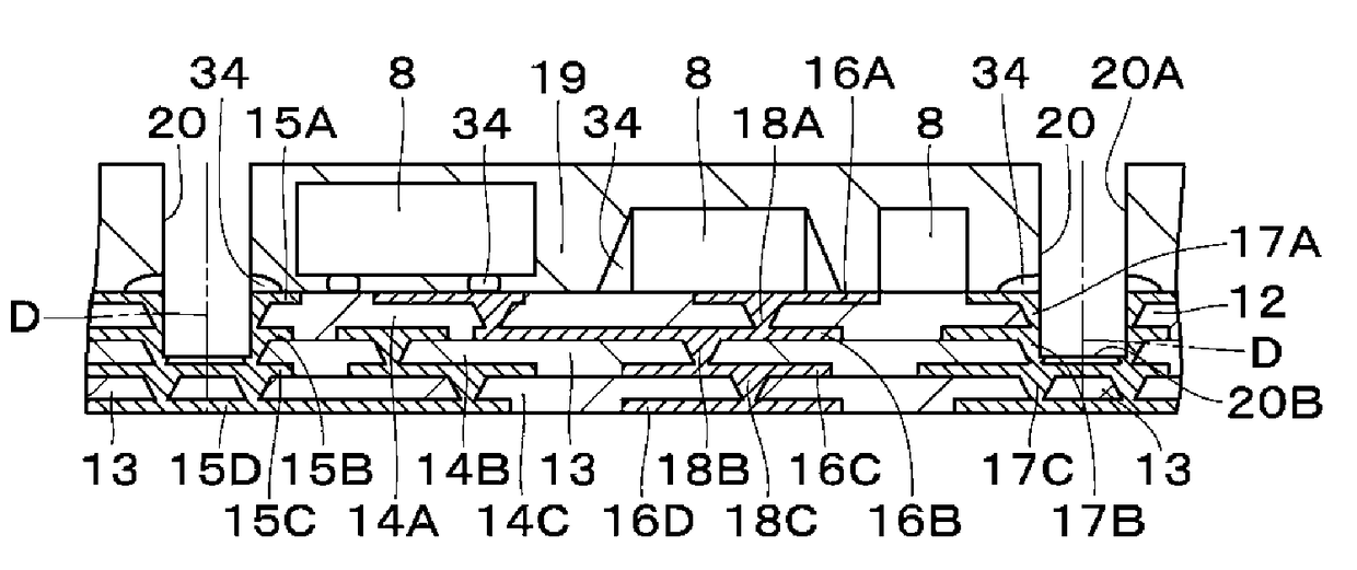
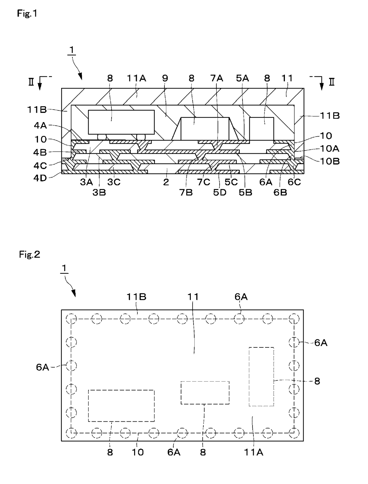
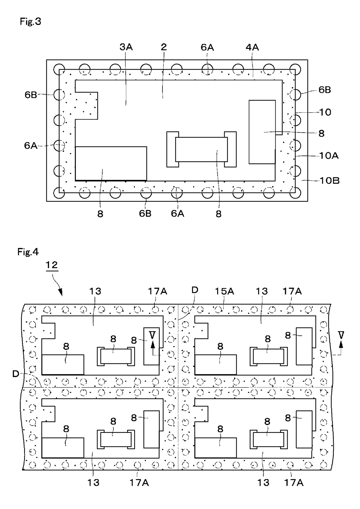
[0035]FIGS. 1 to 9 illustrate a first preferred embodiment of the present invention. A circuit module 1 according to the first preferred embodiment includes a module board 2, electronic components 8, a sealing resin layer 9, a half-cut portion 10, and a shield layer 11.

[0036]The module board 2 includes insulating layers 3A to 3C, ground electrodes 4A to 4D, signal electrodes 5A to 5D, and interlayer vias 6A to 6C and 7A to 7C. The front surface of the module board 2 defines and functions as a component mounting surface on which the electronic components 8 are mounted. The total thickness of the module board 2 is, for example, about 0.1 mm or more and about 1.0 mm or less.

[0037]The module board 2 includes a plurality of insulating layers (for example, three insulating layers) 3A to 3C. The insulating layers 3A to 3C are preferably made of a ther...


PUM


Abstract

A module board includes insulating layers, ground electrodes, signal electrodes, and interlayer vias. Electronic components are mounted on a front surface of the module board, and a sealing resin layer covers the electronic components. A half-cut portion is provided in the module board at an outer peripheral edge thereof and recessed to an intermediate position in a thickness direction of the module board. A shield layer cover the sealing resin layer. The shield layer includes a frame portion that extends into the half-cut portion. The frame portion is electrically connected to ground interlayer vias that are exposed at an end surface and a bottom surface of the half-cut portion.

Description

CROSS REFERENCE TO RELATED APPLICATIONS[0001]This application claims the benefit of priority to Japanese Patent Application No. 2014-127342 filed on Jun. 20, 2014 and is a Continuation application of PCT Application No. PCT / JP2015 / 066755 filed on Jun. 10, 2015. The entire contents of each application are hereby incorporated herein by reference.BACKGROUND OF THE INVENTION[0002]1. Field of the Invention[0003]The present invention relates to a circuit module in which an electronic component is mounted and a method for manufacturing the circuit module.[0004]2. Description of the Related Art[0005]A known circuit module has a structure in which an electronic component is mounted on a surface of a board, an insulating resin is provided so that the electronic component is embedded therein, and the insulating resin is covered with a conductive shield layer (see, for example, Japanese Unexamined Patent Application Publication No. 2004-172176). In such a circuit module, the shield layer reduce...

Claims


Application Information

Patent Timeline
Patent Type & Authority Applications(United States)
IPC IPC(8): H01L25/18H01L23/29H01L21/78H01L23/552H01L25/04H01L23/528H01L21/56H01L23/31
CPCH01L25/18H01L21/561H01L23/29H01L21/78H01L23/552H01L25/04H01L23/5283H01L23/3121H01L23/00H01L23/28H01L23/31H01L23/3135H01L24/97H01L2224/16227H01L2224/97H01L2924/15159H01L2924/15313H01L2924/19105H05K1/0218H05K3/0052H05K3/284H05K2201/0715H05K2203/0228H01L2924/15192H01L2924/19041H01L2924/19042H01L2924/19043H01L2224/81
Inventor HAMADA, SHU
Owner MURATA MFG CO LTD
Why Eureka
Try Eureka