Multi-State Attenuator

a multi-state attenuator and attenuator technology, applied in the field of electronic circuits, can solve the problems of not providing for handling high-power signals, or providing flexibility in design for various applications, and achieves the effects of low insertion loss, minimal effect on chip area and power dissipation, and high input power

Active Publication Date: 2017-04-13
PSEMI CORP
View PDF5 Cites 11 Cited by
  • Summary
  • Abstract
  • Description
  • Claims
  • Application Information

AI Technical Summary

Benefits of technology

[0010]In many applications involving RF signals and in which attenuators are used, it is important to be able to handle high input power but with low insertion loss and parasitic effects, and with minimal effect on chip area and power dissipation on an integrated circuit (IC) die (or “chip”). Such applications include, for example, antenna-transceiver RF signal paths and low noise amplifiers (LNAs) in radio-based systems, such as cellular telephones, WiFi, and the like. The present invention is directed to providing several multi-state attenuator configurations which are capable of handling high power signals, have low insertion loss and parasitic effects, have few or no glitches between state transitions, have minimal effect on chip area and power dissipation on an IC chip, and provide flexibility of design for various applications.

Problems solved by technology

However, a drawback of the circuit type taught in the '323 patent is that it does not provide for handling of high power signals, or provide flexibility of design for various applications.

Method used


Image

  • Multi-State Attenuator
  • Multi-State Attenuator
  • Multi-State Attenuator

Examples


Embodiment Construction

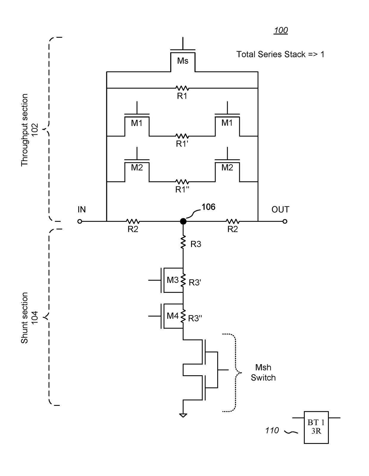
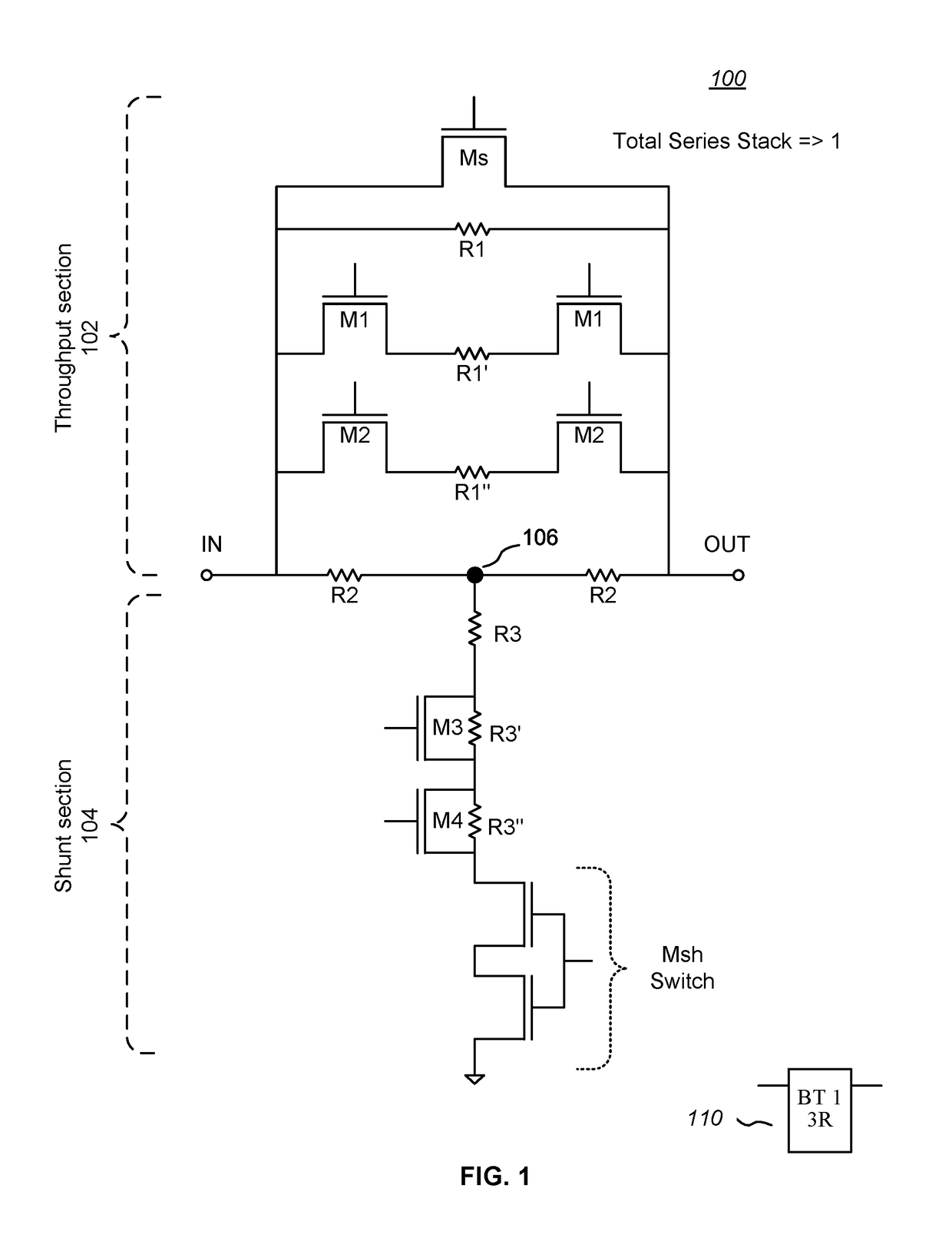
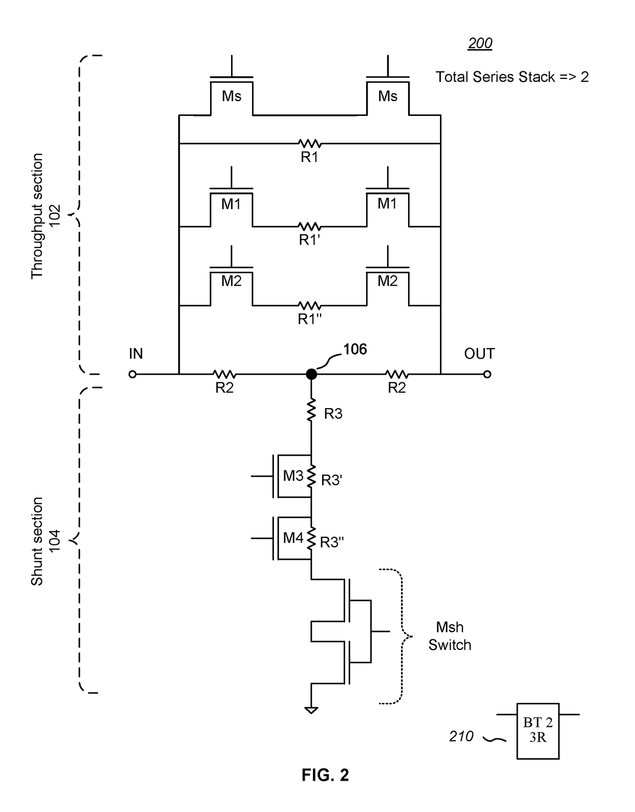
[0032]In many applications involving RF signals and in which attenuators are used, it is important to be able to handle high input power but with low insertion loss and parasitic effects, and with minimal effect on chip area and power dissipation on an integrated circuit (IC) die (or “chip”). Such applications include, for example, antenna-transceiver RF signal paths and low noise amplifiers (LNAs) in radio-based systems, such as cellular telephones, WiFi, and the like. The present invention is directed to providing several multi-state attenuator configurations which are capable of handling high power signals, have low insertion loss and parasitic effects, have few or no glitches between state transitions, have minimal effect on chip area and power dissipation on an IC chip, and provide flexibility of design for various applications.

[0033]More particularly, the present invention includes bridged-T type, pi-type, T-type, and L-pad type multi-state attenuator configurations each havin...


PUM


Abstract

Multi-state radio frequency (RF) attenuator configurations that include bridged-T type, pi-type, and T-type structures each having a programmable throughput section and a coupled programmable shunt section. The throughput sections and shunt sections may be configured in various combinations of parallel and serial fixed or selectable resistance elements such that multiple resistance states and impedance matching states can be programmatically selected, and may include stacked switch elements to withstand applied voltages to a specified design level.

Description

CROSS-REFERENCE TO RELATED APPLICATION—CLAIM OF PRIORITY[0001]This patent application is a continuation application of U.S. patent application Ser. No. 14 / 878,750, filed Oct. 8, 2015 entitled “Multi-State Attenuator”, the disclosure of which is incorporated herein by reference in its entirety.BACKGROUND[0002](1) Technical Field[0003]This invention relates to electronic circuits, and more particularly to multi-state attenuator circuits.[0004](2) Background[0005]An attenuator is an electronic device that reduces the power of a signal without appreciably distorting its waveform. An attenuator is functionally the opposite of an amplifier (although the two work by different methods)—while an amplifier provides gain, an attenuator provides loss (or, equivalently, a gain less than one). Classic examples of radio frequency (RF) attenuators are bridged-T type, pi-type, T-type, and L-pad type attenuators.[0006]A multi-state attenuator may be formed with switched resistive elements for varying...

Claims


Application Information

Patent Timeline
Patent Type & Authority Applications(United States)
IPC IPC(8): H03H11/24
CPCH03H11/245H03H7/25H03K5/08H03K17/687
Inventor SHRIVASTAVA, RAVINDRANATH
Owner PSEMI CORP
Why Eureka
Try Eureka