Distortion Compensation Circuit

a compensation circuit and distortion technology, applied in the direction of amplifiers, amplifiers with semiconductor devices/discharge tubes, amplifier modifications to reduce noise influence, etc., can solve the problems of not improving the inability to improve the linearity of high-power amplifiers using si ldmosfets, so as to achieve the effect of improving the linearity even more efficiently

Inactive Publication Date: 2007-11-15
FURUNO ELECTRIC CO LTD
View PDF4 Cites 9 Cited by
  • Summary
  • Abstract
  • Description
  • Claims
  • Application Information

AI Technical Summary

Benefits of technology

[0027] According to this, it is possible to provide a distortion compensation circuit having the characteristic that only the phase is advanced, while the gain is maintained constant, by selecting the values of the inductor and the resistor, and the constant of the diode. Here, in the multistage high power amplifier using a Si LDMOSFET, the change with respect to increase in input power is more prominent for the phase delay than for the gain decrease, so that it is possible to improve the linearity even more efficiently by combining it with distortion compensation circuits having the characteristic that the gain is increased and the phase is advanced with an increase in input power (for example, the distortion compensation circuits according to the first to fifth aspects of the invention) or distortion compensation circuits in which the gain is increased, while the phase is maintained substantially constant.

Problems solved by technology

In other words, a conventional distortion compensation circuit as described in Non-patent Document 1 that is used for an amplifier using a GaAsFET does not have input-output characteristics that cancel the nonlinearity of a high power amplifier using a Si LDMOSFET, so that it cannot improve the linearity of a high power amplifier using a Si LDMOSFET.
Moreover, as described above, high power amplifiers using a Si LDMOSFET has the characteristic that the phase is temporarily advanced with an increase in input power, although it is eventually delayed.
When the input power is increased beyond such a range, the circuit does not have input-output characteristics that cancel the nonlinearity of a high power amplifier using a Si LDMOSFET, so that it cannot improve the linearity of a high power amplifier using a Si LDMOSFET.

Method used


Image

  • Distortion Compensation Circuit
  • Distortion Compensation Circuit
  • Distortion Compensation Circuit

Examples


embodiment

of Sixth Aspect of the Invention

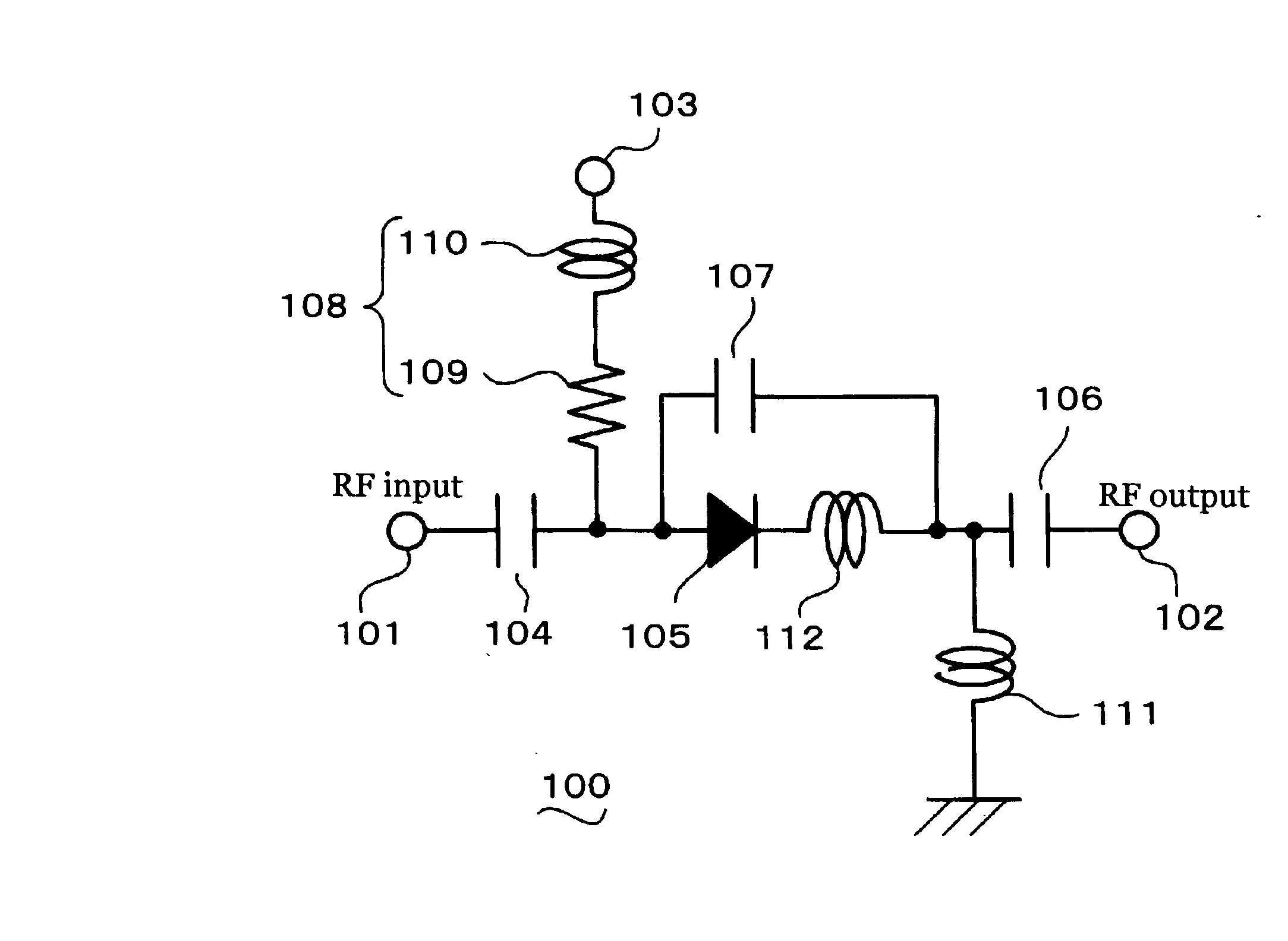
[0092] Next, a distortion compensation circuit according to an embodiment of the sixth aspect of the invention is described below with reference to FIG. 11. FIG. 11 is a circuit diagram showing a distortion compensation circuit according an embodiment of the sixth aspect of the invention.

[0093] As shown in FIG. 11, in a distortion compensation circuit 100 according to an embodiment of the sixth aspect of the invention, a diode 105 directed in the forward direction is connected in series with a signal path between an input terminal 101 and an output terminal 102. In addition, an inductor 112 is connected in parallel with the diode 105. Furthermore, a resistor 113 is connected in parallel with the diode 105. Here, the diode 105 may be any diode whose impedance changes depending on an applied voltage.

[0094] Next, the operation of the distortion compensation circuit 100 according to the embodiment of the sixth aspect of the invention is described. A sig...


PUM


Abstract

There is provided a distortion compensation circuit that can compensate for the nonlinearity of an amplifier having the characteristic that the gain is reduced and the phase is delayed with an increase in input power. An inductor 112 is connected in series with a diode 105 of a distortion compensation circuit 100. The resistance components of the diode 105 decrease with an increase in input power, so that the effect of the impedance of the inductor 112 connected in series with the diode 105 appears, and the impedance of the distortion compensation circuit 100 becomes inductive, producing the characteristic that the phase is advanced. At the same time, the resistance components of the diode 105 decrease with an increase in input power, thus producing the characteristic that the loss is reduced and the gain is increased.

Description

CROSS REFERENCE OF RELATED APPLICATION [0001] PCT Application PCT / JP2005 / 011781 and Japanese Patent Application Tokugan No. 2004-273764 are hereby incorporated by reference. TECHNICAL FIELD [0002] The present invention relates to a distortion compensation circuit that is connected before or after an amplifier for use. BACKGROUND ART [0003] Although it is desirable that an amplifier used for a radio communications system or the like has the input-output characteristics that the gain and phase will not change, amplitude distortion and phase distortion occur in practice as input power is increased. Therefore, as shown in FIG. 18, the linearity of the amplifier is improved by connecting, before or after the amplifier, a distortion compensation circuit having input-output characteristics that cancel the nonlinearity of the amplifier. [0004] Examples of conventional distortion compensation circuits include the technology described in Patent Document 1 or Non-patent Document 1. By way of a...

Claims


Application Information

Patent Timeline
Patent Type & Authority Applications(United States)
IPC IPC(8): H03G3/20
CPCH03F1/3205H03F3/191H03F1/3276H03F1/3241
Inventor KASHIWA, TAKUOOHNISHI, YOSHIFUMI
Owner FURUNO ELECTRIC CO LTD
Why Eureka
Try Eureka