

Semiconductor device and method of manufacturing semiconductor device
a semiconductor and semiconductor technology, applied in the field of semiconductor devices and a manufacturing method of semiconductor devices, can solve the problems of increasing the cost of lithography process and the physical limit of the device dimension, increasing the price of manufacturing apparatus and mask sets, and reducing the cost of chips. , the effect of low cos
- Summary
- Abstract
- Description
- Claims
- Application Information
AI Technical Summary
Benefits of technology
Problems solved by technology
Method used
Image

Examples
first exemplary embodiment
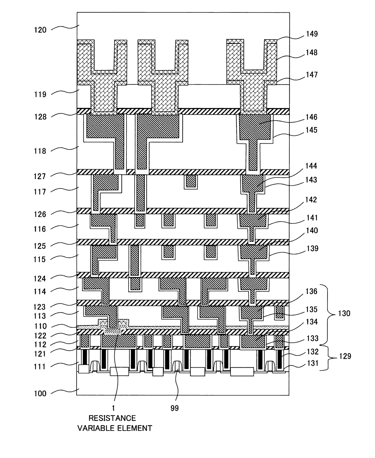
[0068]First, description is given about a semiconductor device and a method of manufacturing the semiconductor device according to a first exemplary embodiment of the present invention. The first exemplary embodiment of the present invention first describes a semiconductor device on which a resistance variable element is mounted, and a method of manufacturing the semiconductor device, and describes how to form a hard copy.
[0069]A reconfigurable circuit to be hard copied in the present invention has a resistance variable element on a semiconductor substrate. The resistance variable element is a type of metal crosslink formation / depletion, and includes a wiring serving as a lower electrode provided with a copper wiring, the copper wiring having an opening part thereon, an ion conductive layer in contact with the opening part, and an upper electrode provided on an upper face of the ion conductive layer. Side and bottom faces of the copper wiring are surrounded by a barrier metal.
[0070]...
example 1
[0101]Next, description is given of a modification example relating to a method of manufacturing a hard copy, as an example 1 of the first exemplary embodiment. FIG. 7(A) is a sectional view illustrating a configuration of a resistance variable element in a reconfigurable circuit, and FIGS. 7(B) and 7(C) are sectional views each illustrating a configuration of an original resistance variable element part at a time of manufacturing a hard copy. FIG. 7(A) illustrates a resistance variable element having the same configuration as the resistance variable element in the reconfigurable circuit in FIG. 6(A). The same reference numerals are assigned to the same components, and description therefor is omitted.
[0102]In the present example, a mask for an opening part to be formed in an insulating barrier film positioned above a copper wiring is changed and a solid electrolyte layer is eliminated from a resistance variable element, at a time of manufacturing a hard copy of a reconfigurable circ...
example 2
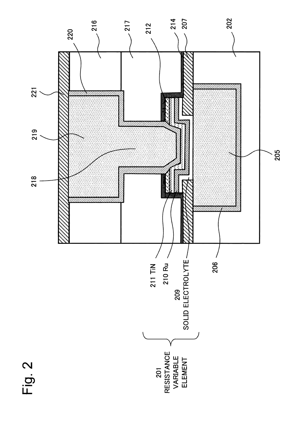
[0106]Next, description is given of another modification example relating to a method of manufacturing a hard copy, as an example 2 of the first exemplary embodiment. FIG. 8(A) is a sectional view illustrating a configuration of a resistance variable element in a reconfigurable circuit, and FIGS. 8(B) and 8(C) are sectional views each illustrating a configuration of an original resistance variable element part at a time of manufacturing a hard copy. A semiconductor device in FIG. 8(A) includes a resistance variable element similar to that in FIG. 3.
[0107]A multi-layered wiring layer includes a pair of first wirings 805a and 805b, a via plug 819, and the resistance variable element. In FIG. 8(A), the pair of first wirings 805a and 805b are lower wirings. The pair of first wirings 805a and 805b also serve as lower electrodes of a three-terminal switch. The resistance variable element is formed by sequentially stacking a solid electrolyte film 809, a Ru film 810, and a TiN film 811. Th...
PUM
 Abstract
Description
Claims
Application Information