Level shift circuit and display driver

a level shift circuit and display driver technology, applied in logic circuits, pulse techniques, instruments, etc., can solve the problems of level shift circuit not working properly in some cases, level shift circuit not working properly, significant increase in circuit amount, etc., to reduce the area occupied by level shift circuit, reduce the effect of current driving capability and increase the operation speed of level shift circui

Active Publication Date: 2017-06-01
LAPIS SEMICON CO LTD
View PDF2 Cites 8 Cited by
  • Summary
  • Abstract
  • Description
  • Claims
  • Application Information

AI Technical Summary

Benefits of technology

[0013]In the present invention, a two-phase level shift is conducted in which an input signal of low amplitude is first converted to a voltage signal of medium amplitude by the first level shift part, and then the voltage signal is converted to a voltage signal of high amplitude by the second level shift part. By converting an input signal of low amplitude to a voltage signal of high amplitude through two phases, it is possible to use transistors with a low current driving capability for the first and second level shift part. This makes it possible to reduce the area occupied by the level shift circuit.
[0014]Furthermore, in each of the first and second level shift parts, a resistance element that causes the current restricting effect is provided on a path of an electric current that flows from the transistor on the higher potential side to the transistor on the lower potential side to restrict a through current in each level shift part. This makes it possible to increase the operation speed of the level shift circuit.

Problems solved by technology

However, even when the above-mentioned level shift circuit includes a diode-connected transistor, if a difference between the amplitude of the input digital signal and the amplitude of the output signal that was subjected to the level shift is significant, the level shift circuit does not function properly in some cases.
That is, because the amplitude of the gate-source voltage of a P-channel transistor that conducts charging is much greater than that of the gate-source voltage of an N-channel transistor that conducts discharging, the capacities of the two transistors differ greatly, and as a result, the level shift circuit does not function properly.
Possible solutions to make the level shift circuit function correctly include increasing the size of the transistors used for this level shift circuit, but this would cause a significant increase in amount of the circuit.

Method used


Image

  • Level shift circuit and display driver
  • Level shift circuit and display driver
  • Level shift circuit and display driver

Examples


embodiment 1

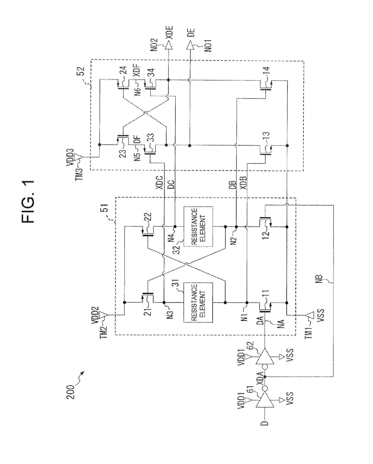
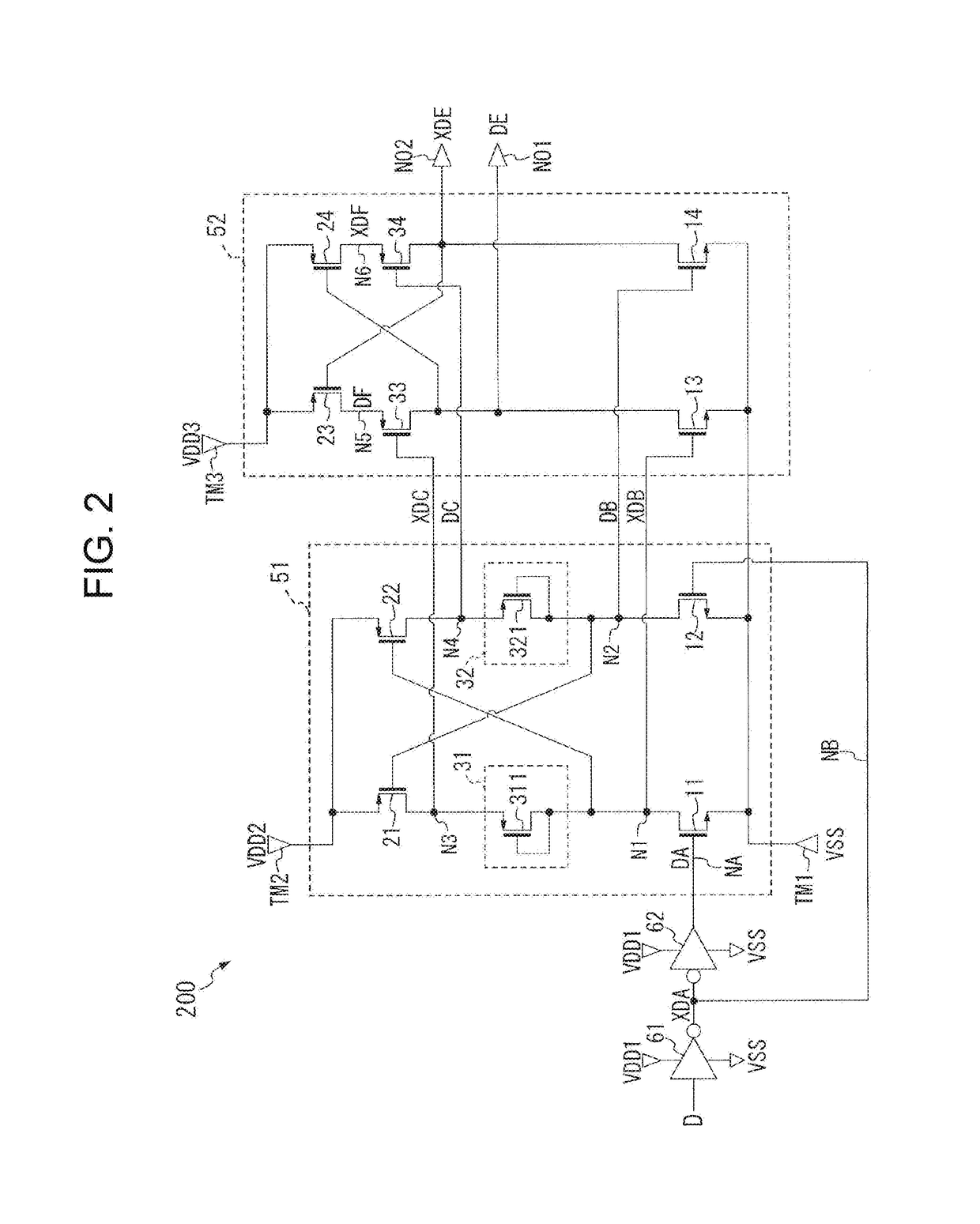
[0045]FIG. 2 is a circuit diagram showing the internal configuration of the level shift circuit 200 of Embodiment 1 of the present invention. The level shift circuit 200 of FIG. 2 is the same as that shown in FIG. 1 except that a P-channel MOS transistor 311 that is diode-connected in which the drain and gate terminals are connected to each other is used in place of the resistance element 31 shown in FIG. 1, and a P-channel MOS transistor 321 that is diode-connected in which the drain and gate terminals are connected to each other is used in place of the resistance element 32. The voltage polarity of each of the low power supply potential VDD1, medium power supply potential VDD2, and high power supply potential VDD3 with respect to the reference power supply potential VSS is positive, and the levels of the respective power supply potentials have the same relationship as that of FIG. 1.

[0046]In the transistor 311, the gate and drain terminals are connected to the node N1, and the sou...

embodiment 2

[0066]FIG. 4 is a circuit diagram showing the internal configuration of the level shift circuit 200 of Embodiment 2 of the present invention.

[0067]In the level shift circuit 200 of FIG. 4, an N-channel MOS transistor 312 is used for the resistance element 31 in place of the P-channel MOS transistor 311, and an N-channel MOS transistor 322 is used for the resistance element 32 in place of the P-channel MOS transistor 321. Other configurations are the same as those of FIG. 2. The relationships of the power supply potentials are the same as those of FIG. 1.

[0068]In the transistor 312, the gate and drain terminals are connected to the node N3, and the source terminal is connected to the node N1. In the transistor 322, the gate and drain terminals are connected to the node N4, and the source terminal is connected to the node N2.

[0069]The transistor 312 is configured such that the potential difference between the nodes N1 and N3 when the operation current flows is equal to or greater than...

embodiment 3

[0071]FIG. 5 is a circuit diagram showing the internal configuration of the level shift circuit 200 of Embodiment 3 of the present invention. In the level shift circuit 200 of FIG. 5, a diode 313 is used for the resistance element 31 in place of the MOS transistors (311,312) and a diode 323 is used for the resistance element 32 in place of the transistors (321, 322). Other configurations are the same as those of FIG. 2.

[0072]In the diode 313, the anode is connected to the node N3 and the cathode is connected to the node N1. In the diode 323, the anode is connected to the node N4 and the cathode is connected to the node N2.

[0073]The diode 313 is configured such that the potential difference between the nodes N1 and N3 when the operation current flows is equal to or greater than the absolute value of the threshold voltage of the P-channel transistor 22, and that the potential difference between the nodes N1 and N3 when the current is shut off is smaller than the absolute value of the ...


PUM


Abstract

A level shift circuit configured to generate an output signal having higher amplitude than that of an input signal. The level shift circuit includes serially-connected first and second level shift circuit for two-step amplitude increase of the input signal. The first level shift circuit includes first to fourth transistors, each of which has a control terminal and first and second current terminals, and first and second resistance elements respectively connected between the first and third transistors, and between the second and fourth transistors. A potential difference between two ends of each resistance element is respectively smaller than, or no smaller than, a respective predetermined potential difference when a current does not flow, or flows, therethrough. The second level shift circuit has fifth to tenth transistors, each of which has a control terminal and first and second current terminals. The output signal is outputted through a connection between the second current terminals of the fifth and ninth transistors.

Description

BACKGROUND OF THE INVENTION[0001]Technical Field[0002]The present invention relates to a level shift circuit that shifts the level of a data signal, and a display driver that includes the level shift circuit.[0003]Background Art[0004]In recent years, active matrix displays using a liquid display device or organic EL element have become the mainstream of display devices. In such display devices, a larger screen, higher resolution, and higher image quality such as improvement of video characteristics are demanded, which is causing an increase in voltage amplitude of a signal (gradation signal) supplied to a display panel by a column driver (display driver) that drives the display panel.[0005]On the other hand, due to the demands for high-speed transfer with a smaller number of wiring lines, lower EMI (electro-magnetic interference), and the like, various control signals and picture data signals supplied from the display controller to the column driver are made to have lower amplitude....

Claims


Application Information

Patent Timeline
Patent Type & Authority Applications(United States)
IPC IPC(8): G09G3/20H03K19/017G11C19/00H03K19/0185
CPCG09G3/2092H03K19/018521H03K19/017G11C19/00G09G2310/0289G09G2330/06G09G2310/0291G09G2300/0809G09G2310/027G09G2300/043G09G2310/0286G09G3/3275G09G3/3685H03K19/018507G09G2310/0275
Inventor TSUCHI, HIROSHI
Owner LAPIS SEMICON CO LTD
Why Eureka
Try Eureka