Thin film transistor substrate and display using the same
Active Publication Date: 2017-06-01
LG DISPLAY CO LTD
View PDF8 Cites 20 Cited by
Summary
Abstract
Description
Claims
Application Information
AI Technical Summary
This helps you quickly interpret patents by identifying the three key elements:
Problems solved by technology
Method used
Benefits of technology
Benefits of technology
The present patent provides a thin film transistor substrate for flat panel display that has two different type transistors on the same substrate. This allows for compensation of any demerits of one type transistor by the other type transistor, especially the thin film transistor with low frequency driving characteristics. This results in a display that has low power consumption and can be used for portable and / or wearable appliances.
Problems solved by technology
However, using the technologies having developed until now, it is restricted to get display having the excellent low power consumption properties.
Method used
Image
Click on the blue label to locate the original text in one second.
Reading with bidirectional positioning of images and text.
Examples
first embodiment
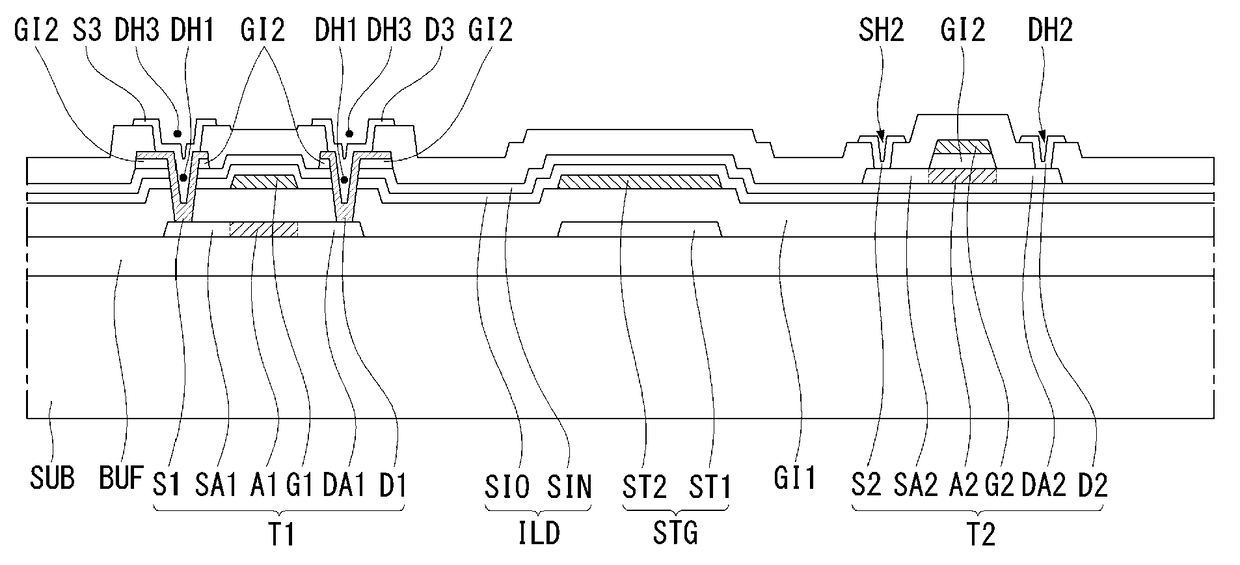
[0044]Referring to FIG. 1, we will explain about the first embodiment of the present disclosure. FIG. 1 is a cross sectional view illustrating a structure of a thin film transistor substrate for a flat panel display in which two different type thin film transistors are formed, according to the first embodiment of the present disclosure. Here, we will explain with the cross sectional views mainly because it clearly shows the main features of the present disclosure, in convenience, the plane view is not used.
[0045]Referring to FIG. 1, the thin film transistor substrate for a flat panel display according to the first embodiment comprises a first thin film transistor T1 and a second thin film transistor T2 which are disposed on the same substrate SUB. The first and second thin film transistors T1 and T2 may be apart far from each other, or they may be disposed within a relatively closed distance. Otherwise these two thin film transistors are disposed as being overlapped each other.
[0046...
second embodiment
[0083]Hereinafter, referring to FIG. 3, we will explain about the second embodiment of the present disclosure. FIG. 3 is a cross sectional view illustrating a structure of a thin film transistor substrate for a flat panel display in which two different type thin film transistors are formed, according to the second embodiment of the present disclosure.
[0084]The thin film transistor substrate according to the second embodiment is basically very similar with that of the first embodiment. The main difference is on a first light shielding layer LS1 for preventing the lights from the outside of the bottom side of the first thin film transistor T1. Further, under the second thin film transistor T2, a second light shielding layer LS2 may be further included for preventing the light incident from outside.
[0085]The first light shielding layer LS1 may be formed by separated mask process, under the buffer layer BUF. The second light shielding layer LS2 may be formed of the same material and at ...
first application example
[0101]The thin film transistor substrate having two different type thin film transistors on the same substrate, above explained, can be applied to various type display including the flat panel display, the flexible display and / or the curved display. Forming the different two type thin film transistors on the same substrate, we can get various merits. Hereinafter, referring to FIG. 5, we will explain how many advanced features and merits can be expected from the thin film transistor substrate according to a first application example of the present disclosure. FIG. 5 is a block diagram illustrating a structure of the display according to a first application example of the present disclosure.
[0102]The first and the second transistors T1 and T2 would be formed in each pixel of the display panel 100 for switching the data voltage applied to the pixel or for driving the pixel. For the case of organic light emitting diode display, the second thin film transistor T2 may be a switch element ...
[0001]This application claims the benefit of Korea Patent Application No. 10-2015-0166448 filed on Nov. 26, 2015, which is incorporated herein by reference for all purposes as if fully set forth herein.BACKGROUND[0002]Field of the Invention[0003]The present disclosure relates to a thin film transistor substrate, and more particularly, to a thin film transistor substrate having two different type thin film transistors on the same substrate, and a method for manufacturing the same.[0004]Discussion of the Related Art[0005]Nowadays, as the information society is developed, the requirements of displays for representing information are increasing. Accordingly, the various flat panel displays (or ‘FPD’) are developed for overcoming many drawbacks of the cathoderay tube (or ‘CRT’) such as heavy weight and bulk volume. The flat panel display devices include the liquid crystaldisplay device (or ‘LCD’), the plasma display panel (or ‘PDP’), the organic light emitting display device (or ‘OLED’...
Claims
Application Information
Patent Timeline
Application Date:The date an application was filed.
Publication Date:The date a patent or application was officially published.
First Publication Date:The earliest publication date of a patent with the same application number.
Issue Date:Publication date of the patent grant document.
PCT Entry Date:The Entry date of PCT National Phase.
Estimated Expiry Date:The statutory expiry date of a patent right according to the Patent Law, and it is the longest term of protection that the patent right can achieve without the termination of the patent right due to other reasons(Term extension factor has been taken into account ).
Invalid Date:Actual expiry date is based on effective date or publication date of legal transaction data of invalid patent.

