

Circuit, semiconductor device, display device, electronic device, and driving method of circuit
- Summary
- Abstract
- Description
- Claims
- Application Information
AI Technical Summary
Benefits of technology
Problems solved by technology
Method used
Image

Examples
embodiment 1
[0098]In this embodiment, an example of a semiconductor device 10 functioning as a grayscale voltage generator circuit will be described.
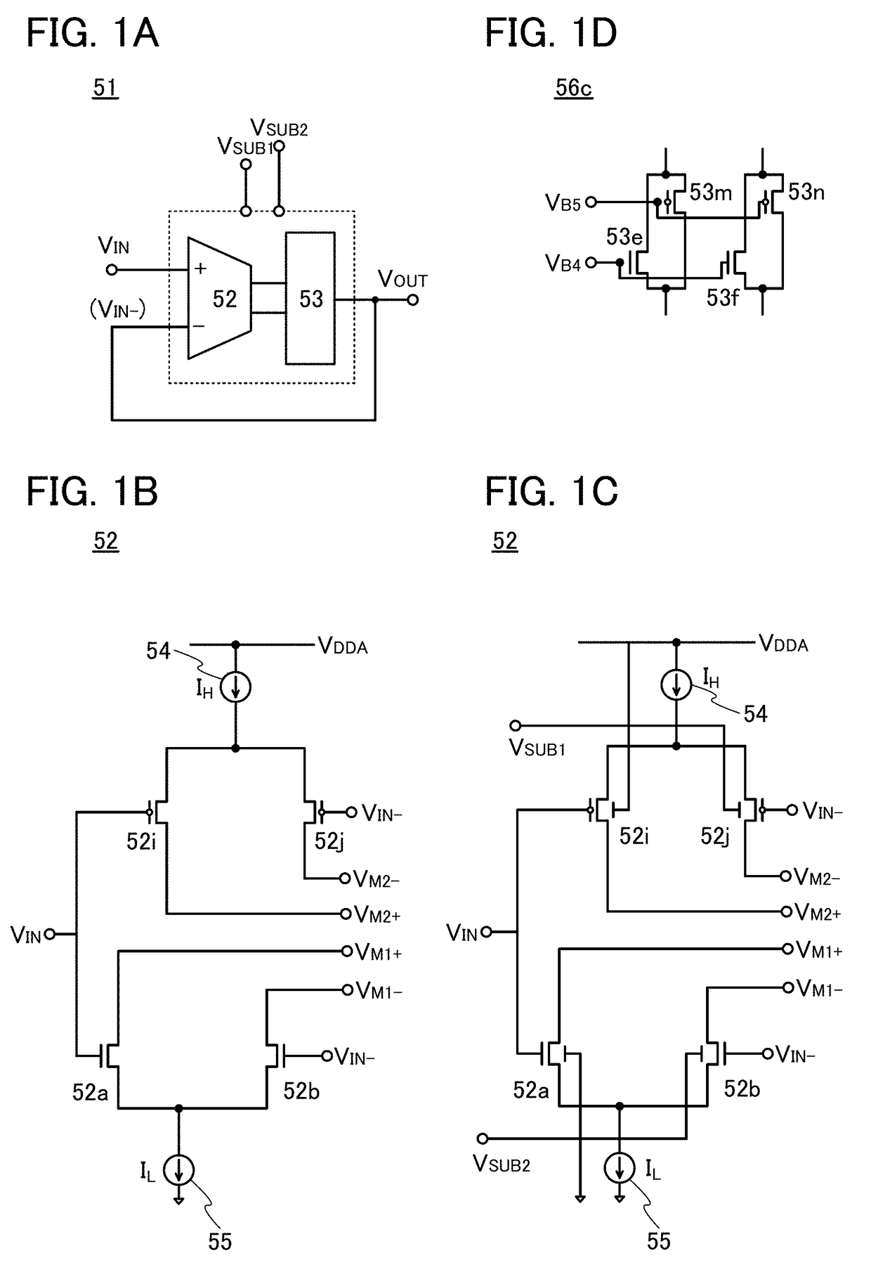
[0099]FIG. 1A illustrates an example of an amplifier circuit 51. The amplifier circuit 51 includes a terminal IN functioning as a non-inverting input terminal, a terminal IN− functioning as an inverting input terminal, and a terminal OUT functioning as an output terminal. A potential VIN is supplied to the terminal IN. A potential VOUT is output from the terminal OUT. The output from the terminal OUT is fed back to the terminal IN−.
[0100]The amplifier circuit 51 includes a terminal SUB1 and a terminal SUB2. A potential VSUB1 and a potential VSUB2 are supplied to the terminal SUB1 and the terminal SUB2, respectively. In the amplifier circuit 51, a value obtained by adding a voltage represented by ΔV to the potential VIN is obtained as the potential VOUT. Here, ΔV is a value controlled by the potentials VSUB1 and VSUB2 input to the amplifier circuit ...
example 1
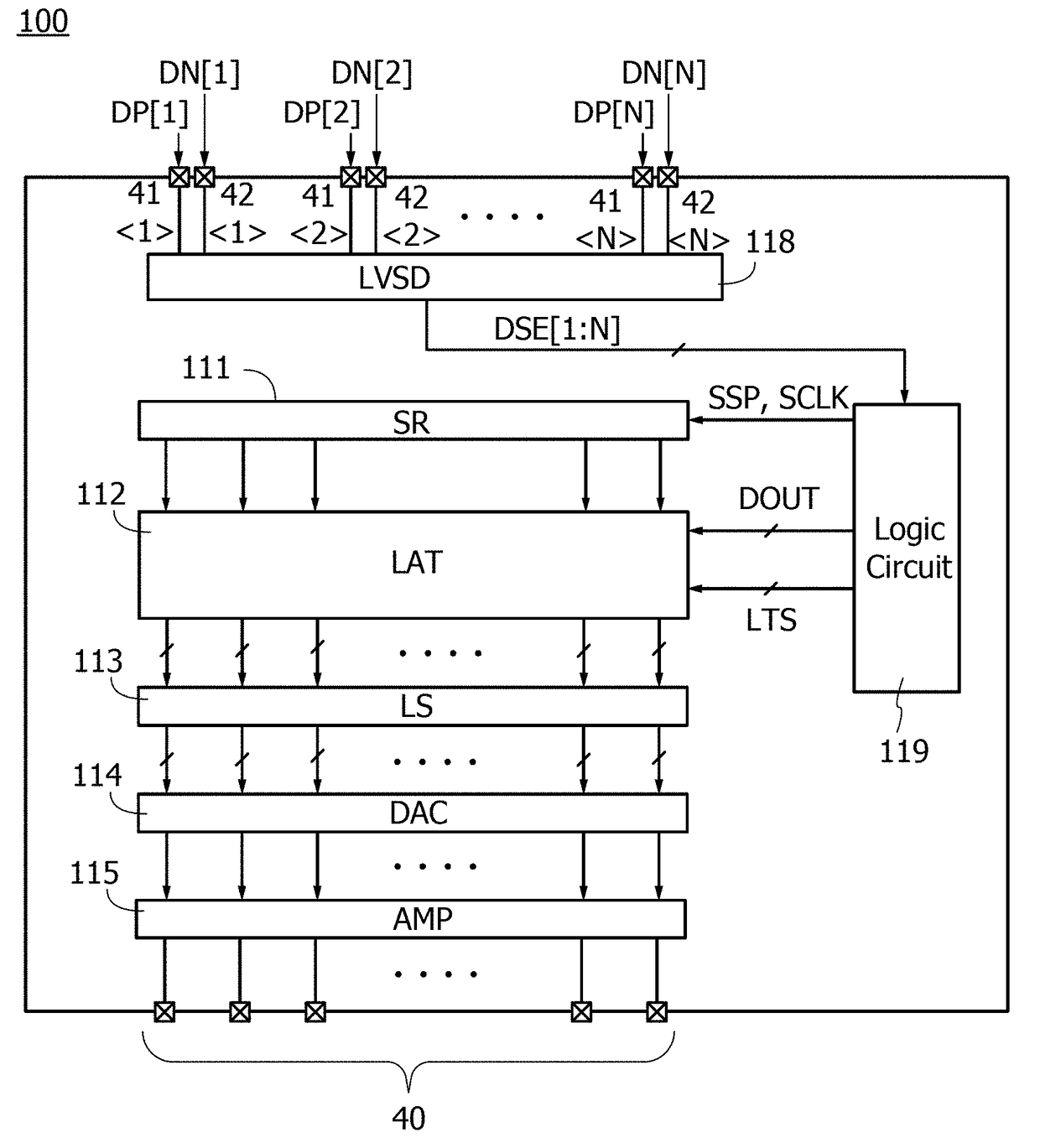
OF SEMICONDUCTOR DEVICE
[0127]The semiconductor device 10 of one embodiment of the present invention includes a digital-to-analog converter circuit (D / A converter circuit) 11, a D / A converter circuit 31, a D / A converter circuit 32, and the amplifier circuit 51. The amplifier circuit 51 includes the amplifier circuit 52 and the amplifier circuit 53.
[0128]The semiconductor device 10 has a function of converting an N-bit image signal (N is a natural number of 2 or more) into an analog signal to output the analog signal. An output of the semiconductor device 10 is output from the terminal OUT as the potential VOUT.
[0129]The D / A converter circuit 11 is a circuit that converts an upper M-bit image signal (such a signal is hereinafter referred to as an upper-bit signal) of the N-bit signal into analog signals. Note that M is a natural number smaller than N. The D / A converter circuit 11 has a function of generating a potential VIN for 2M gray level which corresponds to the upper-bit signal.
[...
example 2
OF SEMICONDUCTOR DEVICE
[0143]FIG. 5 illustrates an example of the semiconductor device 10 which is different from that in FIG. 4. In the semiconductor device 10 illustrated in FIG. 5, the circuit in FIG. 1B is used as the amplifier circuit 52 and the circuit in FIG. 3B is used as the amplifier circuit 53.
[0144]A difference between FIG. 4 and FIG. 5 is described. In FIG. 4, the potential VSUB1 is supplied to the second gate or the substrate potential of the transistor 52j and the potential VSUB2 is supplied to the second gate or the substrate potential of the transistor 52b, whereas, in FIG. 5, the potential VSUB1 is supplied to the second gate or the substrate potential of the transistor 53j and the potential VSUB2 is supplied to the second gate or the substrate potential of the transistor 53a.
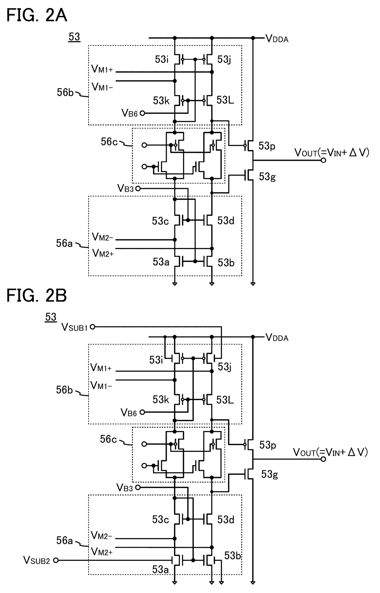
[0145]A pair of the transistor 53j and the transistor 53i in the amplifier circuit 53 in FIG. 5 is described. The first gate of the transistor 53i and the first gate of the transistor 53j are...
PUM
 Abstract
Description
Claims
Application Information