Method for Forming an Alignment Layer of a Liquid Crystal Display Device and Display Device Manufactured Thereby

Active Publication Date: 2017-07-20
OMNIVISION TECH INC
View PDF7 Cites 1 Cited by
  • Summary
  • Abstract
  • Description
  • Claims
  • Application Information

AI Technical Summary

Benefits of technology

[0011]The present invention overcomes the problems associated with the prior art by providing a novel method for forming the alignment layer(s) of a liquid crystal display device by annealing alignment layer material (e.g., spin-on diele

Problems solved by technology

One common limitation of polyimide alignment layers is that they are not very stable under high intensity and/or prolonged illumination.
Indeed, after tens of hours of light stress, polyimide alignment layers can degrade enough to cause flares (e.g., unwanted lighter areas) in the displayed images.
And, after several hundred hours of light stress, the degradation is severe enough to cause permanent black areas in a displayed white image and/or permanent white areas in a black image.
In other words, light stress wil

Method used


Image

  • Method for Forming an Alignment Layer of a Liquid Crystal Display Device and Display Device Manufactured Thereby
  • Method for Forming an Alignment Layer of a Liquid Crystal Display Device and Display Device Manufactured Thereby
  • Method for Forming an Alignment Layer of a Liquid Crystal Display Device and Display Device Manufactured Thereby

Examples


Embodiment Construction

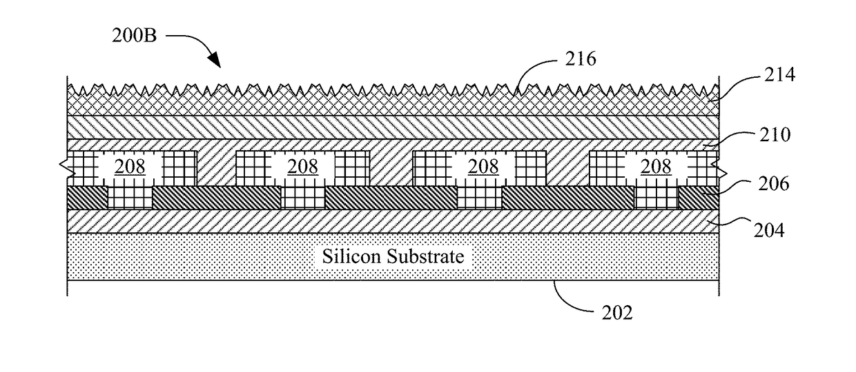
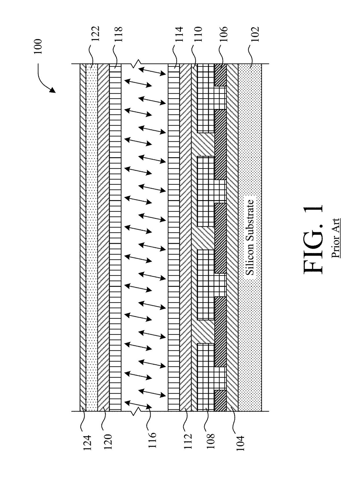
[0036]The present invention overcomes the problems associated with the prior art by providing a new method for forming the alignment layer(s) of a liquid crystal display device by annealing a spin-on dielectric with laser light. Accordingly, the liquid crystal display devices of the invention feature alignment layer(s) that are very stable under prolonged, high-intensity light stress and that are easily and inexpensively manufactured with high throughput. In the following description, numerous specific details are set forth (e.g., particular laser scan traces, laser specifics, etc.) in order to provide a thorough understanding of the invention. Those skilled in the art will recognize, however, that the invention may be practiced apart from these specific details. In other instances, details of well-known wafer-processing practices (e.g., spin-on processes, wafer preparation processes, etc.) and components (e.g., wafer processing apparatuses, etc.) have been omitted, so as not to unn...


PUM


Abstract

A novel method of forming an alignment layer of a liquid crystal display device includes the steps of providing a substrate (e.g., a processed silicon wafer, etc.) having an alignment layer material deposited thereon and applying a series of pulses from a pulse laser to anneal portions of the alignment layer material and alter its surface morphology. The method can include the step of depositing the alignment layer material (e.g., a spin-on dielectric including SiO2) over the substrate using a spin-on process prior to laser annealing. Applying the series of laser pulses creates a repetitive pattern of features that facilitate alignment of liquid crystals according to a laser scan trace. Liquid crystal display devices with laser-annealed alignment layer(s) are also disclosed. The alignment layers of the invention are quickly and inexpensively applied and are very robust under prolonged, high-intensity light stress.

Description

BACKGROUND[0001]Field of the Invention[0002]This invention relates generally to liquid crystal display (LCD) devices and methods of manufacturing them. Even more particularly the invention relates to methods for forming alignment layers used in LCD displays.[0003]Description of the Background Art[0004]Reflective and transmissive LCD devices are used in video projectors, rear projection televisions, computer displays, and other devices as a means for producing high-quality imagery. FIG. 1 shows a known liquid crystal display device 100, which in this embodiment, is a reflective liquid crystal on silicon (LCOS) light valve. Display device 100 is formed on a silicon substrate 102, and includes integrated circuitry 104, an insulating layer 106, a plurality of pixel mirrors 108, a planarized layer 110, a protective coating 112, a lower liquid crystal alignment layer 114, a liquid crystal layer 116, an upper liquid crystal alignment layer 118, a transparent electrode layer 120, a transpar...

Claims


Application Information

Patent Timeline
IPC IPC(8): G02F1/1337G02F1/1343
CPCG02F1/13378G02F2001/133776G02F1/133734G02F1/13439G02F1/133788G02F1/136
Inventor QIAN, YINTAI, DYSON HSIN-CHIHZHANG, MINGMIAO, CHIA-CHUN
Owner OMNIVISION TECH INC
Why Eureka
Try Eureka