Magnetic Field Sensor Using In Situ Solid Source Graphene and Graphene Induced Anti-Ferromagnetic Coupling and Spin Filtering

a magnetic field sensor and solid source technology, applied in the direction of magnetic measurements, magnetic bodies, thin material processing, etc., can solve the problem of low sensitivity (%/oe) and the response is not strong enough

Active Publication Date: 2017-08-24
THE UNITED STATES OF AMERICA AS REPRESENTED BY THE SECRETARY OF THE NAVY
View PDF3 Cites 1 Cited by
  • Summary
  • Abstract
  • Description
  • Claims
  • Application Information

AI Technical Summary

Problems solved by technology

Hall sensors are cheap and have a linear r

Method used


Image

  • Magnetic Field Sensor Using In Situ Solid Source Graphene and Graphene Induced Anti-Ferromagnetic Coupling and Spin Filtering
  • Magnetic Field Sensor Using In Situ Solid Source Graphene and Graphene Induced Anti-Ferromagnetic Coupling and Spin Filtering
  • Magnetic Field Sensor Using In Situ Solid Source Graphene and Graphene Induced Anti-Ferromagnetic Coupling and Spin Filtering

Examples


example 1

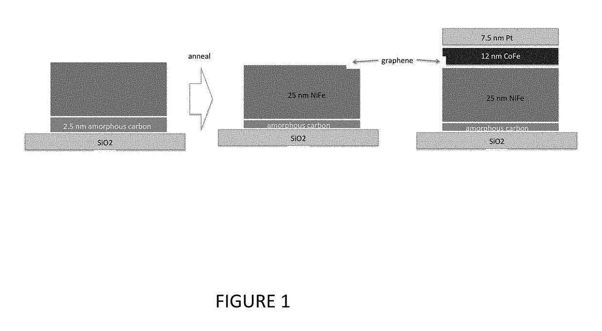
[0018]The full stack was prepared in situ using DC magnetron sputtering in an AJA sputtering chamber with base pressure less than 3×10⁻⁸ Torr. The sputtering guns were in a confocal geometry with ˜15 degree of incidence angle and ˜15 cm of distance between substrate and the gun.

[0019]The substrate, Silicon wafers with a 27.5 nm of thermal oxide, were ultrasonically cleaned 15 minutes each in acetone then alcohol. After loading, the substrate was back sputtered for three minutes at 10W, 100V in 20 mTorr of Argon. 2.5 nm of amorphous carbon was grown at a rate of 0.31 nm per minute at 100 W in 3 mTorr of Ar. 25 nm of Ni80Fe20 was grown at 0.05 nm / sec at 100 W in 3 mTorr Ar.

example 2

[0020]An in situ anneal at 875 C. for 10 minutes was performed in a pressure below 2×10⁻⁶ Torr. The sample was then allowed to cool down to room temperature at 10 C. / min. After the sample was cooled down it was either unloaded for analysis or a layer of 12 nm Co90Fe10 was sputter deposited and capped with 7.5 nm of Pt, see FIG. 1.

[0021]FIG. 5 shows the 4 point resistance of the un-processed film. Four probes were place 1 mm apart and a Current Source was used to supply current to the outer contacts, while the potential difference between the two inner contacts was measured by a Keithley 2000 voltmeter in a standard four-probe electrical measurement. The normalized resistance versus magnetic field is shown in FIG. 5.

[0022]FIG. 5A illustrates a standard four probe resistance measurement on the unprocessed film, probe distance is 1 mm and the applied field is parallel to the current direction. A normalized magneto resistance curve showing a negative 4% effect, inset shows Magnetoresist...


PUM


Abstract

A magnetic field sensor based on two anti-ferromagnetically coupled magnetic layers separated by multilayer graphene, prepared in a single sputter chamber without a vacuum break.

Description

[0001]This application claims priority to and the benefits of U.S. Patent Application No. 62 / 297,550 filed on Feb. 19, 2016, the entirety of which is herein incorporated by reference.BACKGROUND[0002]Magnetic field sensors are ubiquitous, they are found as position, rotation and velocity sensors in vehicles and industrial equipment. They are also used for current sensing in high power applications and the advance in magnetic sensors has enabled the low-cost high-density hard disk industry.[0003]For magnetic sensors to be attractive they need to have a high magnetoresistance (MR>100%), have a linear response in a small magnetic field (% / Oe), and have low resistance (high signal to noise).[0004]Presently, magnetic sensors have high magnetoresistance (MR>100%), for example MgO based magnetic tunnel barriers, but these have a high resistance due to the nature of the tunnel barrier. Hall sensors are cheap and have a linear response but a very low sensitivity (% / Oe). Anisotropic magn...

Claims


Application Information

Patent Timeline
IPC IPC(8): G01R33/09G01R33/00
CPCG01R33/0052G01R33/093H01F10/30H01F10/3254H01F10/3272Y10T428/1114
Inventor VAN 'T ERVE, OLAF M. J.COBAS, ENRIQUECHENG, SHU-FANJONKER, BEREND T.
Owner THE UNITED STATES OF AMERICA AS REPRESENTED BY THE SECRETARY OF THE NAVY
Why Eureka
Try Eureka