

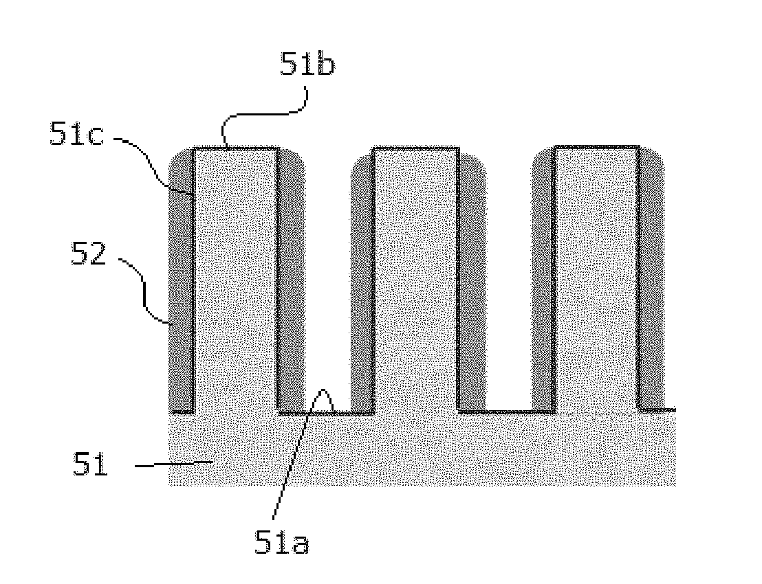
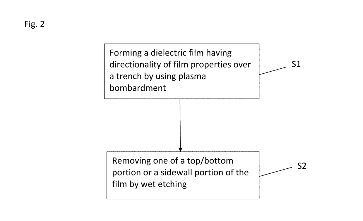
Method for forming silicon nitride film selectively on sidewalls or flat surfaces of trenches
a technology of silicon nitride and selective forming, which is applied in the direction of coating, chemical vapor deposition coating, coating, etc., can solve the problems of reducing affecting so as to improve the quality of the film, reduce the density of the film, and improve the effect of plasma-enhanced chemical vapor deposition
- Summary
- Abstract
- Description
- Claims
- Application Information
AI Technical Summary
Benefits of technology
Problems solved by technology
Method used
Image

Examples
example 1
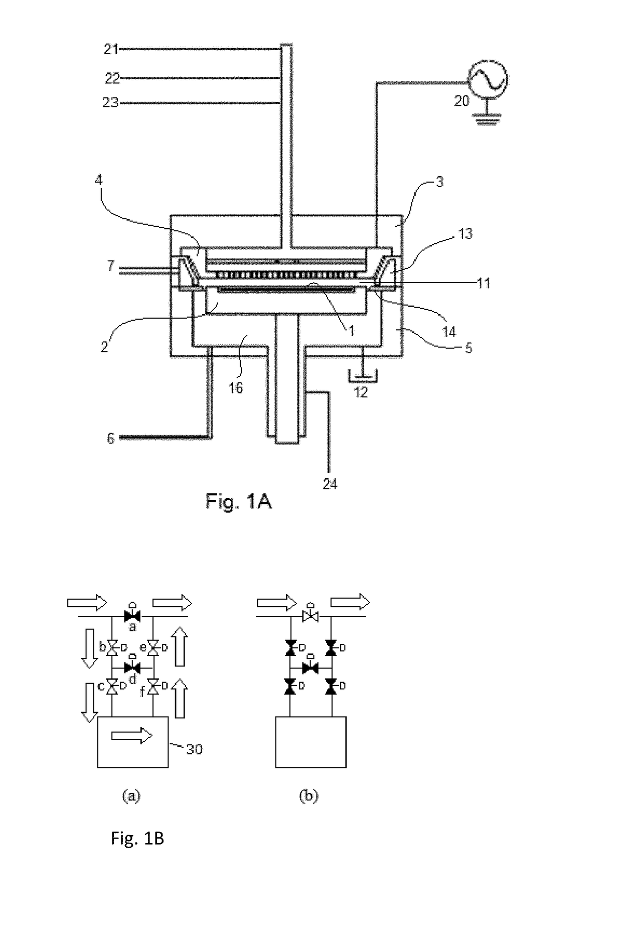
[0078]A SiN film was formed on a Si substrate (Φ300 mm) having trenches by PEALD, one cycle of which was conducted under the conditions shown in Table 4 (deposition cycle) below using the PEALD apparatus illustrated in FIG. 1A and a gas supply system (FPS) illustrated in FIG. 1B.
[0079]After taking out the substrate from the reaction chamber, the substrate was subjected to wet etching under the conditions shown in Table 4 below.
TABLE 4(numbers are approximate)Conditions for Deposition CycleSubstrate temperature400° C.Pressure350 PaPrecursorSiI2H2Precursor pulse0.3 secPrecursor purge0.5 secReactantN2Flow rate of reactant (continuous)2000 sccmFlow rate of carrier gas (continuous)2000 sccm N2Flow rate of dilution gas (continuous)0 sccmRF power (13.56 MHz) for aVariable (see Fig. 7)300-mm waferRF power pulse3.3 secPurge0.1 secGrowth rate per cycle (on top surface)0.05 nm / cycleNumber of cycles (thickness of film on200 times (10 nm)top surface)Step coverage (side / top; side / bottom)100%; 100...
example 2
[0082]The SiN films were deposited under the conditions shown in Table 5, where the threshold RF power was determined to be approximately 400 W in the same manner as in Example 1. The SiN films were then subjected to wet etching under the conditions shown in Table 5. FIG. 8 shows Scanning Transmission Electron Microscope (STEM) photographs of cross-sectional views of the silicon nitride films. As can be seen from FIG. 8, when RF power was 700 W, the top / bottom portions of the film were selectively removed by wet etching, and substantially no film remained (no residual film was observed) on the top surface and at the bottom of the trench. When RF power was 500 W, the top / bottom portions of the film were more predominantly removed than was the sidewall portion of the film by wet etching, but residual film remained on the top surface and at the bottom of the trench, whereas the sidewall portion of the film mostly remained. When RF power was 300 W, the sidewall portion of the film was m...
example 3
[0083]The SiN film was deposited in the same manner as in Example 1 except that RF power was 880W. The SiN film was then subjected to wet etching under the same conditions as in Example 1. FIG. 9 shows a Scanning Transmission Electron Microscope (STEM) photograph of a cross-sectional view of the SiN film after the wet etching. As can be seen from FIG. 9, substantially no film remained (no residual film was observed) on the top surface and at the bottom of the trench.
PUM
| Property | Measurement | Unit |
|---|---|---|
| Thickness | aaaaa | aaaaa |
| Temperature | aaaaa | aaaaa |
| Fraction | aaaaa | aaaaa |
Abstract
Description
Claims
Application Information