Compound micro-transfer-printed optical filter device

a technology of optical filter and micro-transfer, which is applied in the direction of semiconductor devices, instruments, electrical devices, etc., can solve the problems of increasing the elapsed manufacturing time, increasing the waste of materials and time, and increasing the waste of processing time, so as to reduce the amount of wasted optical filter material, reduce the time required for making the integrated component, and the effect of high density of optical filter

Active Publication Date: 2017-08-24
X CELEPRINT LIMITED
View PDF7 Cites 4 Cited by
  • Summary
  • Abstract
  • Description
  • Claims
  • Application Information

AI Technical Summary

Benefits of technology

[0011]The present invention provides advantages over optical filter and light sensor assemblies of the prior art. According to embodiments of the present invention, a much higher density of optical filters is achieved by forming the optical filters over a filter substrate. This reduces the amount of wasted optical filter material. Furthermore, by micro-transfer printing the optical filters over a light transducer, multiple optical filters can be provided without requiring multiple, sequential deposition and patterning of optical filter layers, greatly reducing the time required to make the integrated component. Furthermore, different processes optimized for different materials can be used to make the various optical filters and the semiconductor substrate, optical transducer, and active circuit, improving their performance.
[0012]Embodiments of the present invention therefore enable compound optical filter devices comprising a variety of different heterogeneous materials that can each be processed or assembled separately using different, possibly incompatible, processes and at higher densities, thereby reducing costs and improving performance. By micro-transfer printing multiple, different optical filters onto a substrate having corresponding multiple optical transducers, manufacturing cycle time and costs are reduced and higher performance enabled.

Problems solved by technology

However, this process is very wasteful, since only the portion of the optical filter layer materials that remains after lift-off or that pass through the shadow mask is used.
Furthermore, the process is sequential, as the light sensor must be made first before the optical filter is applied over the light sensor, increasing the elapsed manufacturing time.
Thus, if multiple optical filters are formed on a common substrate, the deposition process must be repeatedly and sequentially performed, leading to further waste in materials and time.

Method used


Image

  • Compound micro-transfer-printed optical filter device
  • Compound micro-transfer-printed optical filter device
  • Compound micro-transfer-printed optical filter device

Examples


Embodiment Construction

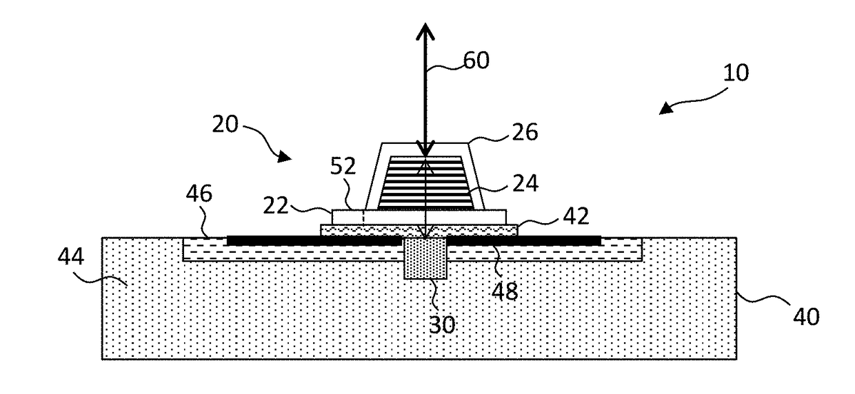
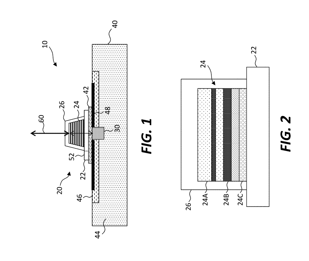
[0067]Referring to the cross section of FIG. 1, a compound optical filter device 10 comprises a semiconductor substrate 40 having an optical transducer 30 formed in or on the semiconductor substrate 40. The optical transducer 30 is responsive to light 60 (e.g., incident light illuminating the optical transducer 30) to produce a signal or is responsive to a signal to emit light 60. An optical filter 20 comprises an optical filter substrate 22 separate, distinct, and independent from the semiconductor substrate 40 and one or more optical filter layers 24 disposed on the optical filter substrate 22. The optical filter device is a compound optical filter device 10 because it incorporates two different substrates (e.g., the semiconductor substrate 40 and the optical filter substrate 22). In certain embodiments, the two different substrates include two different materials. The two different materials can have different attributes, can be processed separately, or can be process incompatibl...


PUM


Abstract

Embodiments of the present invention provide a compound optical filter device comprising a semiconductor substrate having an optical transducer formed on the semiconductor substrate, the optical transducer responsive to light to produce a signal or responsive to a signal to emit light. An optical filter comprises a filter substrate separate and independent from the semiconductor substrate and one or more optical filter layers disposed on the filter substrate. The filter substrate is micro-transfer printed on or over the semiconductor substrate or on layers formed over the semiconductor substrate and over the optical transducer to optically filter the light to which the optical transducer is responsive or to optically filter the light emitted by the optical transducer. In further embodiments, the optical filter is an interference filter and the semiconductor substrate includes active components that can control or operate the optical transducer.

Description

FIELD OF THE INVENTION[0001]The present invention relates to an integrated heterogeneous optical filter device constructed using micro-transfer printing.BACKGROUND OF THE INVENTION[0002]Electro-optical circuits are widely used in communication and sensing devices. In particular, optical filters that rely upon layers of alternating materials having different refractive indices providing constructive and destructive optical interference are widely used. Such filters can transmit or reflect particular frequency ranges of electromagnetic radiation.[0003]Proximity sensors are sensors that detect nearby objects and are commonly used in smartphones and for industrial applications to measure the distance between machine components. In one implementation, proximity sensors include a light emitter and a light sensor that senses the light emitted and measures the time between light emission and sensing light reflected from an object to determine a distance to the object that depends on the spe...

Claims


Application Information

Patent Timeline
Patent Type & Authority Applications(United States)
IPC IPC(8): H01L31/0232H01L33/58
CPCH01L31/0232H01L2933/0058H01L33/58G02B5/28H01L31/02165H01L31/173
Inventor BOWER, CHRISTOPHERCOK, RONALD S.
Owner X CELEPRINT LIMITED
Why Eureka
Try Eureka