

Defect observation apparatus
a technology of defect observation and apparatus, which is applied in the field of defect observation apparatus, can solve the problems of discrepancy between the coordinate system of the sem and the coordinate system of another inspection apparatus, and the mix of defects, so as to reduce the amount of reflected light/scattered light generated from defects, increase the integration degree of semiconductor devices, and reduce the effect of defect siz
- Summary
- Abstract
- Description
- Claims
- Application Information
AI Technical Summary
Benefits of technology
Problems solved by technology
Method used
Image

Examples
embodiment 1
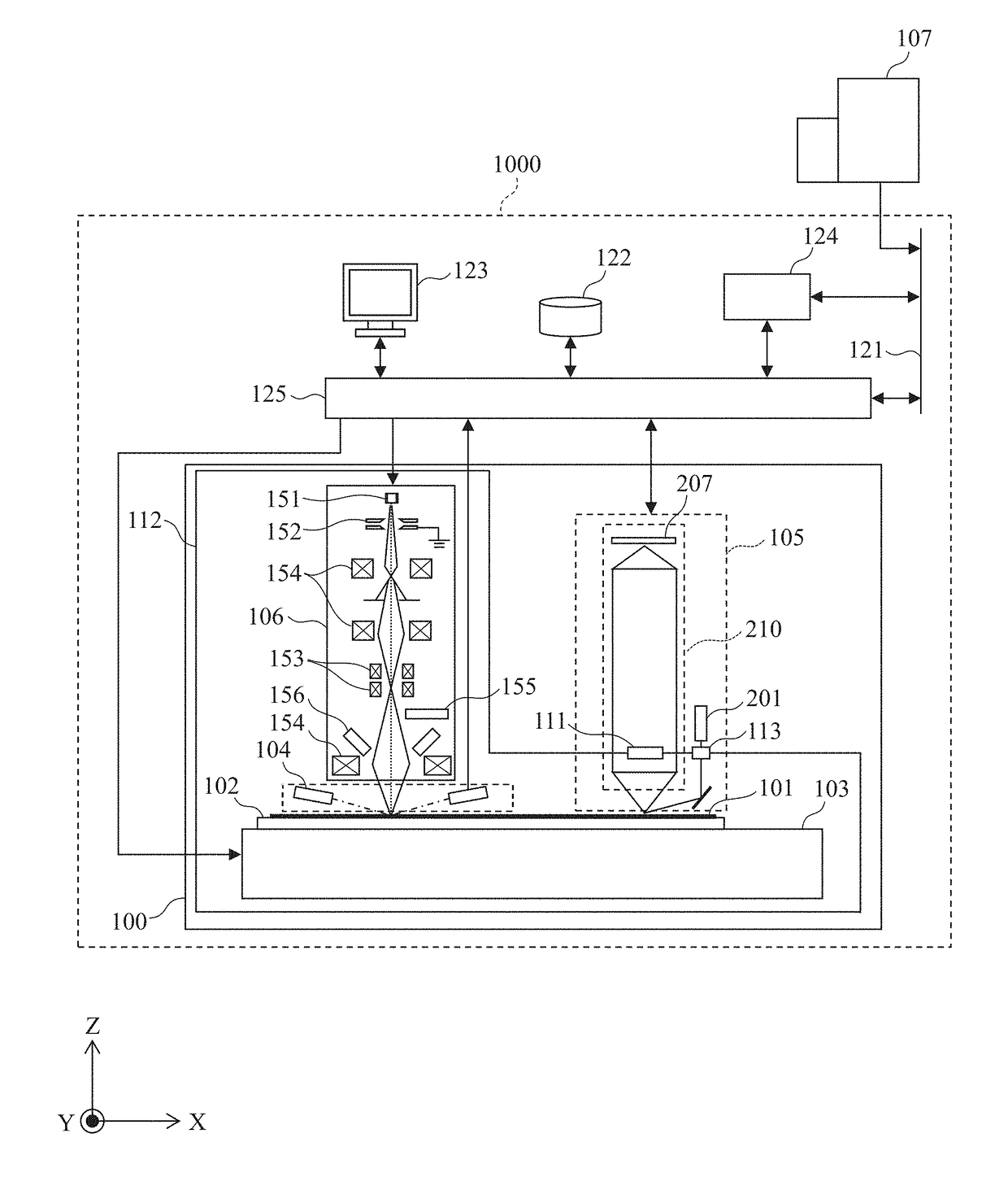
[0032]FIG. 1 is a configuration diagram of a defect observation apparatus in Embodiment 1. A defect observation apparatus 1000 mainly includes a reviewing device 100, a network 121, a database 122, a user interface 123, a storage device 124, and a control unit 125.
[0033]The defect observation apparatus 1000 is connected to a defect inspection apparatus 107, which is an external inspection apparatus, over the network 121. The defect inspection apparatus 107 detects defects on a sample 101 and acquires defect information. The defect information is information about a plurality of defects on the sample 101, and includes information such as a defect ID of each defect, the position coordinates of each defect, and the size of each defect. The defect inspection apparatus 107 may be any device as long as it can acquire information about defects on the sample 101.
[0034]The control unit 125 and the storage device 124 are connected to the defect inspection apparatus 107 over the network 121. D...
embodiment 2
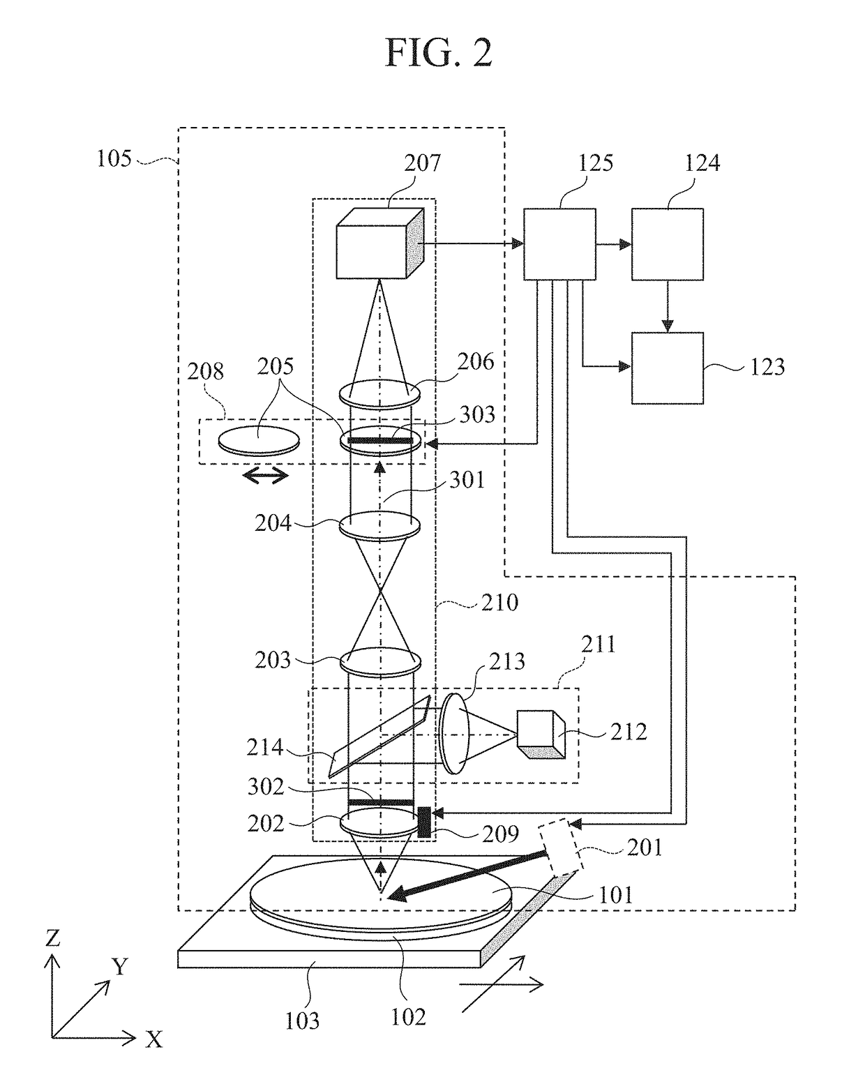
[0129]Next, Embodiment 2 will be described. As the configuration of the reviewing device in this embodiment is the same as that in FIGS. 1 to 3, the description thereof is omitted herein. This embodiment is characterized in that when an image acquired with the optical microscope unit 105 contains a plurality of defects, an ID of each defect in the image can be identified.
[0130]A case where the field of view contains a plurality of defects will be described with reference to FIG. 6. Defect coordinates included in the defect information of the defect inspection apparatus 107 include a detection error 404 of the defect inspection apparatus 107 and link coordinate accuracy 403 between the defect inspection apparatus 107 and the reviewing device 100. A region 401 imaged by the optical microscope unit 105 is a narrow region of about several 100 μm. For example, in the case of the wide-field mode, the field of view has a size of 200 μm×200 μm, while in the case of the high-sensitivity mode...
embodiment 3
[0168]Next, Embodiment 3 will be described. As the configuration of the reviewing device in this embodiment is the same as that in FIGS. 1 to 3, the description thereof is omitted herein. This embodiment is characterized in that when it is determined that an image captured with the optical microscope unit 105 may contain a plurality of defects and there may also be a great difference in luminance between the defects, defect coordinates can be derived from the image of the optical microscope unit 105.
[0169]A case where the field of view contains a plurality of defects and the difference in luminance between the defects is greater than a predetermined value will be described with reference to FIG. 11.
[0170]Suppose that when there is a great difference in size between defects that are close to each other, the inspection mode and imaging conditions are adjusted to those for a defect 1101 with a smaller size (hereinafter referred to as a smaller defect). In such a case, as shown in an im...
PUM
| Property | Measurement | Unit |
|---|---|---|
| elevation angle | aaaaa | aaaaa |
| size | aaaaa | aaaaa |
| size | aaaaa | aaaaa |
Abstract
Description
Claims
Application Information