3D Printed Electronics Using Directional Plasma Jet

a technology of directional plasma jet and 3d printing, which is applied in the direction of additive manufacturing processes, manufacturing tools, coatings, etc., can solve the problems of difficult task of precise thickness control of three-dimensional and/or 3d printed objects, and achieve precise thickness control, precise thickness and aspect ratio control

Active Publication Date: 2017-09-14
UNIVERSITIES SPACE RES ASSOC
View PDF1 Cites 16 Cited by
  • Summary
  • Abstract
  • Description
  • Claims
  • Application Information

AI Technical Summary

Benefits of technology

[0013]Adding printed electronics capability to additive manufacturing will widen the scope of 3D printing technology enabling applications ranging from aerospace to automobiles to medical implants. Site selective deposition of conducting, semiconducting films and other electronic materials with precise thickness control on a three dimensional and / or 3D printed object is a challenging task. For any given 3D electronic printing process, the successful integration depends on its ability to coat conformally with precise thickness and aspect ratio control on a range of substrates, planar or non-planar surfaces, complex non-conformal objects, un-even macroscopic roughness surface, bends, sharp edges etc. Hence, a process that is compatible with 3D printing and a process that meets all the desired characteristics mentioned above is required for successful integration of electronics in the 3D printed structure.

Problems solved by technology

Site selective deposition of conducting, semiconducting films and other electronic materials with precise thickness control on a three dimensional and / or 3D printed object is a challenging task.

Method used


Image

  • 3D Printed Electronics Using Directional Plasma Jet
  • 3D Printed Electronics Using Directional Plasma Jet
  • 3D Printed Electronics Using Directional Plasma Jet

Examples


Embodiment Construction

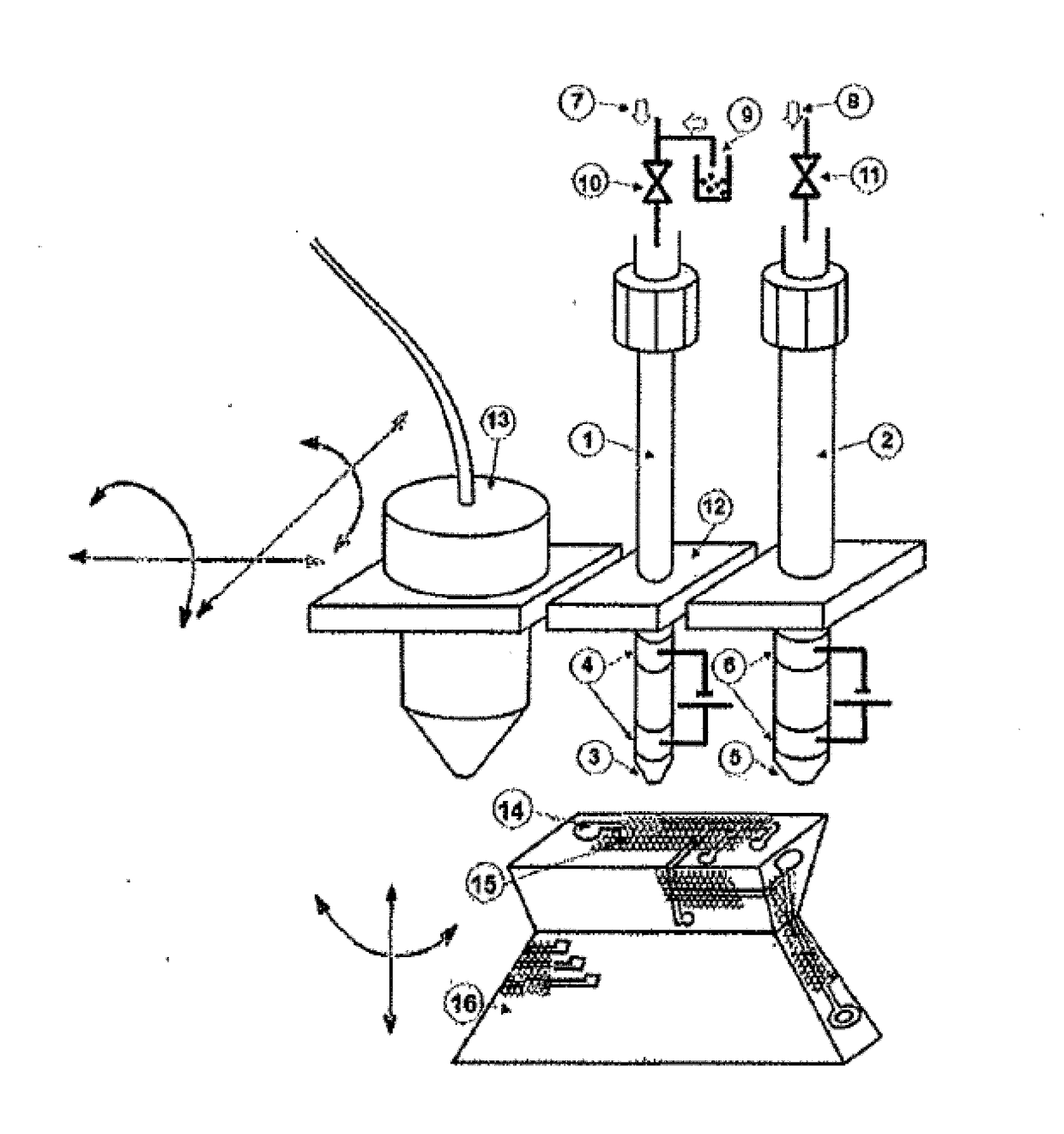
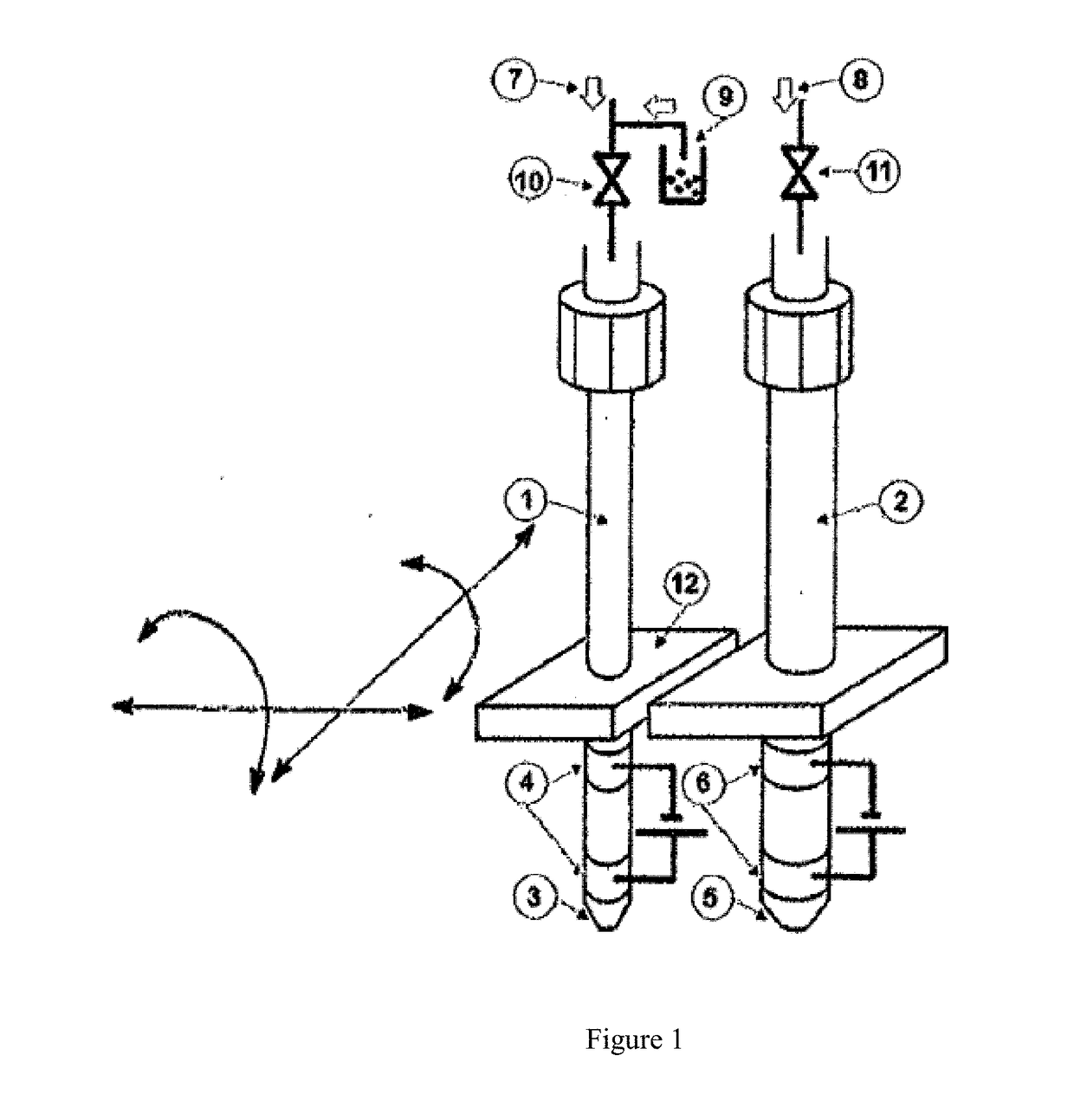
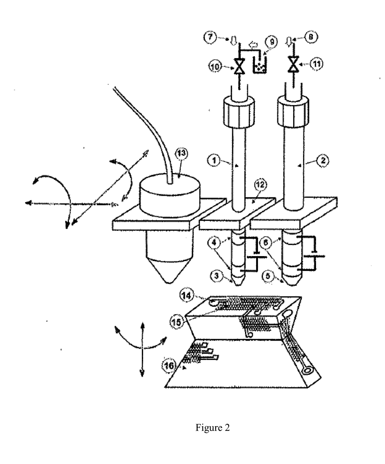
[0048]A central feature of this invention is an additive manufacturing process using an integrated layer-by-layer 3D plasma jet printing of electronic materials, that is, using a highly directional, direct write plasma jet process for depositing electronic materials, with precise thickness and aspect ratio control, on a 3D printed object to create electronic devices using a 3D printer. Unlike any other printing process, 3D plasma jet printing process of the present invention enables controlling of material properties. Unlike any other additive manufacturing technology, this plasma jet printing enables non-gravity based directional printing, controlled jointly by electric field and atmospheric plasma that could be used for printing in any direction by moving the print head rather than moving the substrate to be coated. Another unique feature of the invention is that the same plasma jet used for printing can be used for site selective post deposition treatment of deposited materials b...


PUM

PropertyMeasurementUnit
widthaaaaaaaaaa
widthaaaaaaaaaa
diameteraaaaaaaaaa

Abstract

A device and method for printing 3D articles including electronic and functional elements including 3D printer and a plasma jet printer based on a dielectric barrier atmospheric pressure plasma jet system in which both printing and in-situ treatment and post-deposition treatment can be carried out to tailor the materials characteristics. Plasma jet printer comprising of electrodes in the nozzle/print head for applying electric field and generating atmospheric plasma that could be used for non- gravity based highly directional printing in any direction. Integration of dielectric barrier plasma printer and plasma treatment jets with the 3D printer increases the capability of embedding high performance electronics in a 3D printed structure aiding in additive manufacturing of functional devices. Ability to use a range of materials for print head assembly including micro machined silicon increases the resolution of the plasma jet printer to sub-micron level.

Description

BACKGROUND OF THE INVENTION[0001]Field of the Invention[0002]This invention relates to the field of additive printing.[0003]Description of the Background[0004]Additive manufacturing, also known as 3D printing, using plastic, metals, ceramic, biomaterials, biological materials is revolutionizing manufacturing industries with endless applications. Additive manufacturing using the above mentioned materials individually are well developed. However, additive manufacturing that integrates printing of two or more different materials like plastic, ceramic, metal etc., to form a single end product with desired features is yet to be developed. For example, 3D printing of electronic components on plastics, metals or biomaterials to manufacture an electronic device is severely limited with the type of materials to be used and the compatibility with the process adopted. Imparting electrical properties (semiconducting, metallic, dielectric etc.) to 3D printed objects as an inline manufacturing pr...

Claims


Application Information

Patent Timeline
Patent Type & Authority Applications(United States)
IPC IPC(8): B29C67/00B33Y50/02C23C4/134B33Y30/00
CPCB29C67/0074C23C4/134B33Y50/02B33Y30/00B29C64/106B29C64/188B22F2202/13B22F2999/00B22F12/82B22F10/60B22F12/53B22F12/70B22F12/22B22F12/55B22F10/50B22F10/25B22F3/16B29C64/321B33Y70/00B29C64/209B29C64/205
Inventor GANDHIRAMAN, RAMPRASADMEYYAPPAN, MEYYAKOEHNE, JESSICA E.
Owner UNIVERSITIES SPACE RES ASSOC
Why Eureka
Try Eureka