Non-volatile memory device and method of operating the same

a non-volatile, memory device technology, applied in the direction of digital storage, redundant data error correction, instruments, etc., can solve the problems of increasing the number of defective memory cells, increasing the coupling interference between adjacent memory cells, and losing stored data, so as to improve the performance of the non-volatile memory device, the effect of reducing the read time and the read tim

Active Publication Date: 2017-09-21
SAMSUNG ELECTRONICS CO LTD
View PDF0 Cites 41 Cited by
  • Summary
  • Abstract
  • Description
  • Claims
  • Application Information

AI Technical Summary

Benefits of technology

[0012]The non-volatile memory device and the method of operating the non-volatile memory device according to example embodiments may enhance performance of the non-volatile memory device by separating or independently performing the ECC decoding and the de-randomizing. The seed values may be stored while the ECC decoding is performed to perform the de-randomizing using the stored seed values, and thus the read time may be reduced.
[0013]In addition, according to the result of the ECC decoding, only the correction bits may be stored in the page buffer circuit whereas the rest of bits may be maintained in the page buffer circuit, and thus the read time and the power consumption may be reduced.

Problems solved by technology

Volatile memory devices, such as dynamic random access memory (DRAM) devices, are typically configured to store data by charging or discharging capacitors in memory cells, and lose the stored data when power is off.
As integration degree of semiconductor memory devices increases, the number of defective memory cells increases and coupling interference between adjacent memory cells also increases.
Such increase of the defective memory cells and the coupling interference results in decrease of yield of semiconductor memory devices.

Method used


Image

  • Non-volatile memory device and method of operating the same
  • Non-volatile memory device and method of operating the same
  • Non-volatile memory device and method of operating the same

Examples


Embodiment Construction

[0040]Various example embodiments will be described more fully hereinafter with reference to the accompanying drawings, in which some example embodiments are shown. In the drawings, like numerals refer to like elements throughout. The repeated descriptions may be omitted.

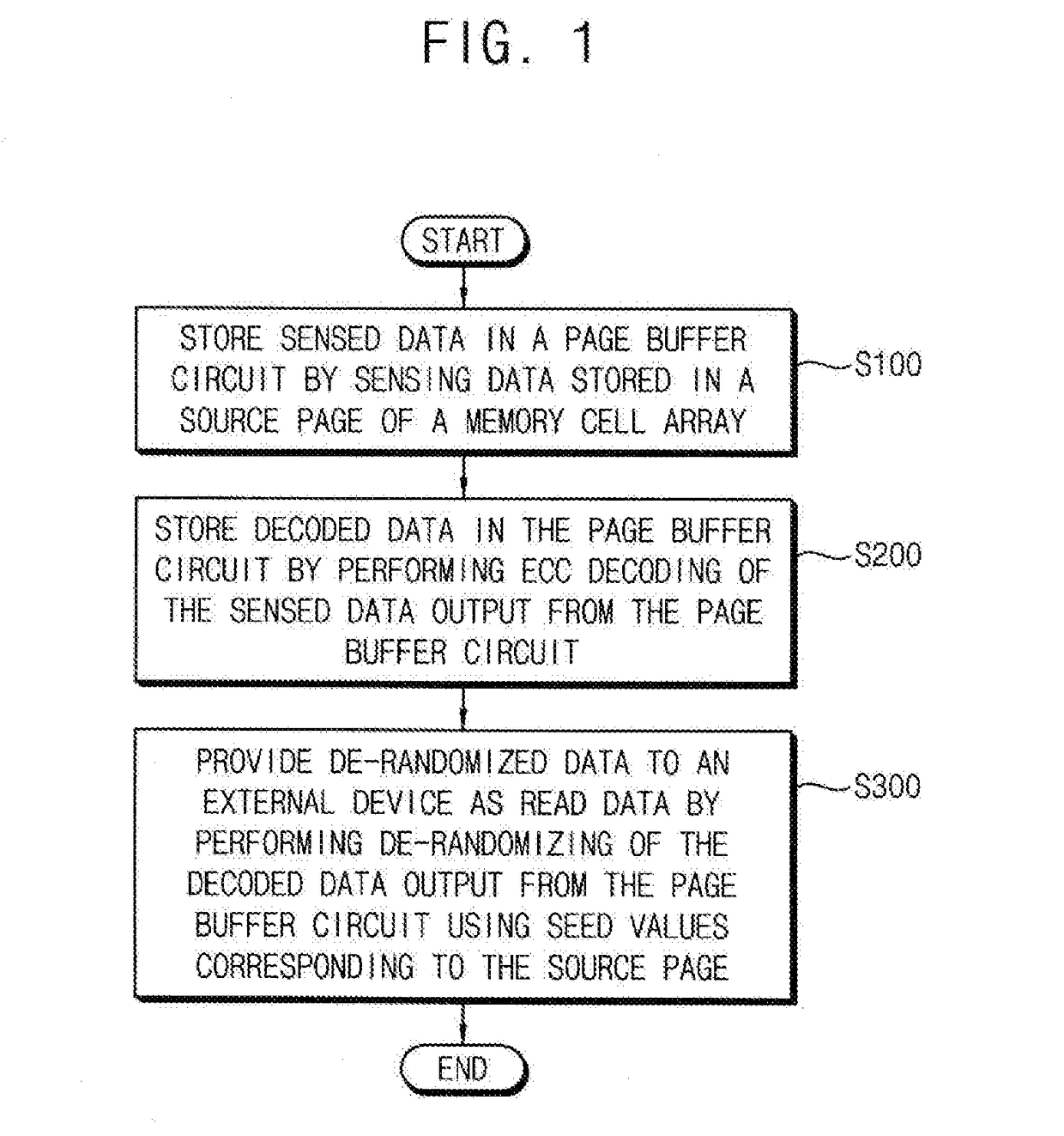
[0041]FIG. 1 is a flow chart illustrating a method of operating a non-volatile memory device according to example embodiments.

[0042]A method corresponding to a read operation of a non-volatile memory device is illustrated in FIG. 1. Referring to FIG. 1, sensed data are stored in a page buffer circuit by sensing data stored in a source page of a memory cell array (S100). Decoded data are stored in the page buffer circuit by performing error correction code (ECC) decoding of the sensed data from the page buffer circuit (S200). Herein, the error correction code (ECC) may be referred to as an error check and correction (ECC). De-randomized data are provided to an external device as read data by performing de-randomizing...


PUM


Abstract

A method of operating a non-volatile memory device, includes, storing sensed data in a page buffer circuit by sensing data stored in a source page of a memory cell array, outputting the sensed data from the page buffer circuit, performing error correction code (ECC) decoding of the sensed data output from the page buffer circuit, storing the decoded data in the page buffer circuit, and providing de-randomized data to an external device as read data by performing de-randomizing of the decoded data output from the page buffer circuit using seed values corresponding to the source page.

Description

CROSS-REFERENCE TO RELATED APPLICATION[0001]This U.S. Non-provisional application claims priority under 35 USC §119 to Korean Patent Application No. 10-2016-0031999, filed on Mar. 17, 2016, in the Korean Intellectual Property Office (KIPO), the disclosure of which is incorporated by reference in its entirety herein.BACKGROUND[0002]1. Technical Field[0003]Example embodiments relate generally to semiconductor integrated circuits, and more particularly to a non-volatile memory device and a method of operating a non-volatile memory device to efficiently perform randomizing and de-randomizing.[0004]2. Discussion of the Related Art[0005]Semiconductor memory devices for storing data may be classified into volatile memory devices and non-volatile memory devices. Volatile memory devices, such as dynamic random access memory (DRAM) devices, are typically configured to store data by charging or discharging capacitors in memory cells, and lose the stored data when power is off. Non-volatile mem...

Claims


Application Information

Patent Timeline
Patent Type & Authority Applications(United States)
IPC IPC(8): G06F11/10G11C29/52
CPCG06F11/1072G11C29/52G06F11/1068G06F11/1044G11C11/161G11C13/0002G11C13/0021G11C2029/0411
Inventor SUNWOO, JUNG
Owner SAMSUNG ELECTRONICS CO LTD
Why Eureka
Try Eureka