Wavelength conversion member, backlight unit, and liquid crystal display device

a technology of wavelength conversion and backlight unit, which is applied in the field of wavelength conversion members, backlight units, liquid crystal display devices, can solve the problems of low film strength, low brightness of backlight units or liquid crystal display devices incorporating wavelength conversion members, and decrease in light extraction efficiency of clusters, etc., and achieve high emission efficiency and sufficient strength

Active Publication Date: 2017-09-28
FUJIFILM CORP
View PDF2 Cites 22 Cited by
  • Summary
  • Abstract
  • Description
  • Claims
  • Application Information

AI Technical Summary

Benefits of technology

[0011]As a result of investigation, the present inventors found that, in a case where the quantum dot concentration in clusters is increased in order to increase the content of quantum dots in a wavelength conversion layer, the emission efficiency of the quantum dots decreases, and the brightness of a backlight unit into which the wavelength conversion member is incorporated decreases. In order to increase the content of quantum dots in a wavelength conversion layer, it is preferable to increase the density of clusters including quantum dots in the wavelength conversion layer rather than to increase the quantum dot concentration in the clusters.
[0012]As a result of a thorough investigation, the present inventors found that spherical clusters can be obtained by, for example, mixing and stirring a liquid mixture of quantum dots and amino silicone corresponding to a ligand material with a monomer material such as epoxy as it is to form an emulsion. However, in a case where a monomer is cured to form a film after the formation of clusters, amino silicone as a cluster portion is liquid as it is. Therefore, the strength of the film is low, and it was found that, in a case where the density of the clusters is increased, a wavelength conversion layer is likely to break. As described below, from the viewpoint of preventing deterioration of quantum dots, it is preferable that opposite surfaces of a wavelength conversion layer are in contact with barrier films. However, in a case where the wavelength conversion layer is likely to break, the adhesive strength between the barrier films and the wavelength conversion layer decreases, and the barrier films are likely to peel off.
[0015]As a result of further investigation, the present inventors found that a wavelength conversion member including spherical clusters and having a high strength can be obtained by adding a polymerizable compound to amino silicone, for example, mixing and stirring the mixture with a monomer material to form an emulsion, and curing both a cluster portion and a monomer portion, thereby completing the present invention.
[0046]According to the present invention, the spherical first cured product including the quantum dots is dispersed in the second cured product. As a result, a wavelength conversion member which has a sufficient strength despite a small thickness of the wavelength conversion layer and having a high emission efficiency can be provided.

Problems solved by technology

However, in a case where clusters including quantum dots are unstructured, the light extraction efficiency from the clusters decreases, and there is a problem in that the brightness of a backlight unit or a liquid crystal display device into which the wavelength conversion member is incorporated decreases.
Therefore, the strength of the film is low, and it was found that, in a case where the density of the clusters is increased, a wavelength conversion layer is likely to break.
However, in a case where the wavelength conversion layer is likely to break, the adhesive strength between the barrier films and the wavelength conversion layer decreases, and the barrier films are likely to peel off.

Method used


Image

  • Wavelength conversion member, backlight unit, and liquid crystal display device
  • Wavelength conversion member, backlight unit, and liquid crystal display device
  • Wavelength conversion member, backlight unit, and liquid crystal display device

Examples


examples

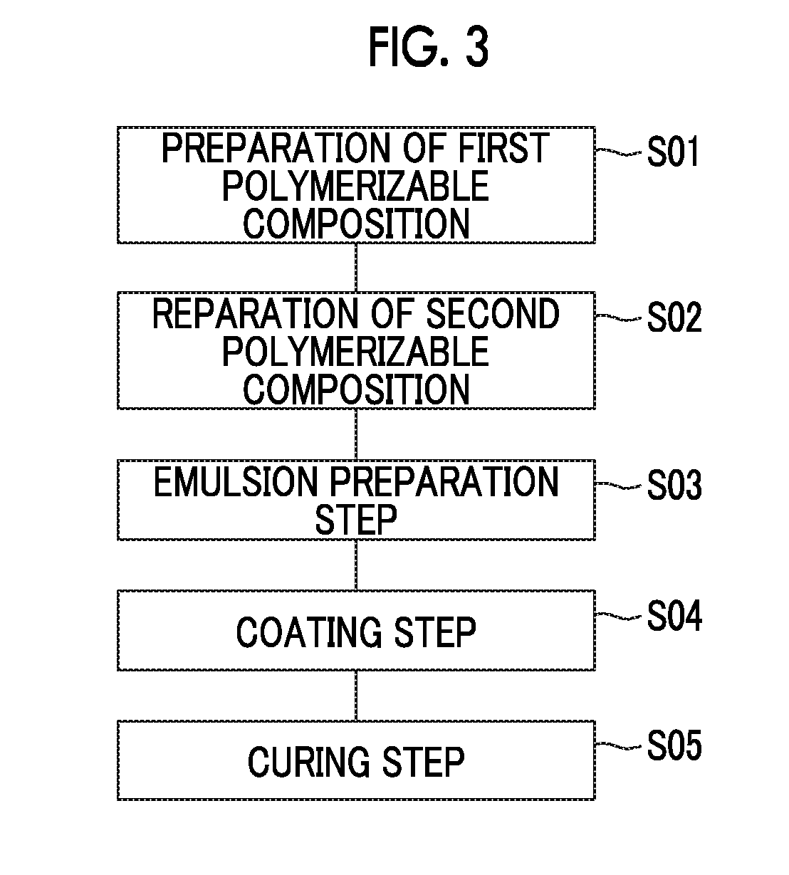
[0241]Hereinafter, the present invention will be described in detail using examples. Materials, used amounts, ratios, treatment details, treatment procedures, and the like shown in the following examples can be appropriately changed within a range not departing from the scope of the present invention. Accordingly, the scope of the present invention is not limited to the following specific examples.

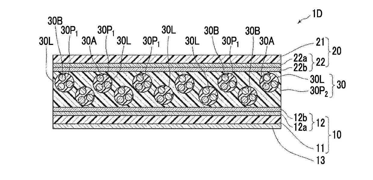
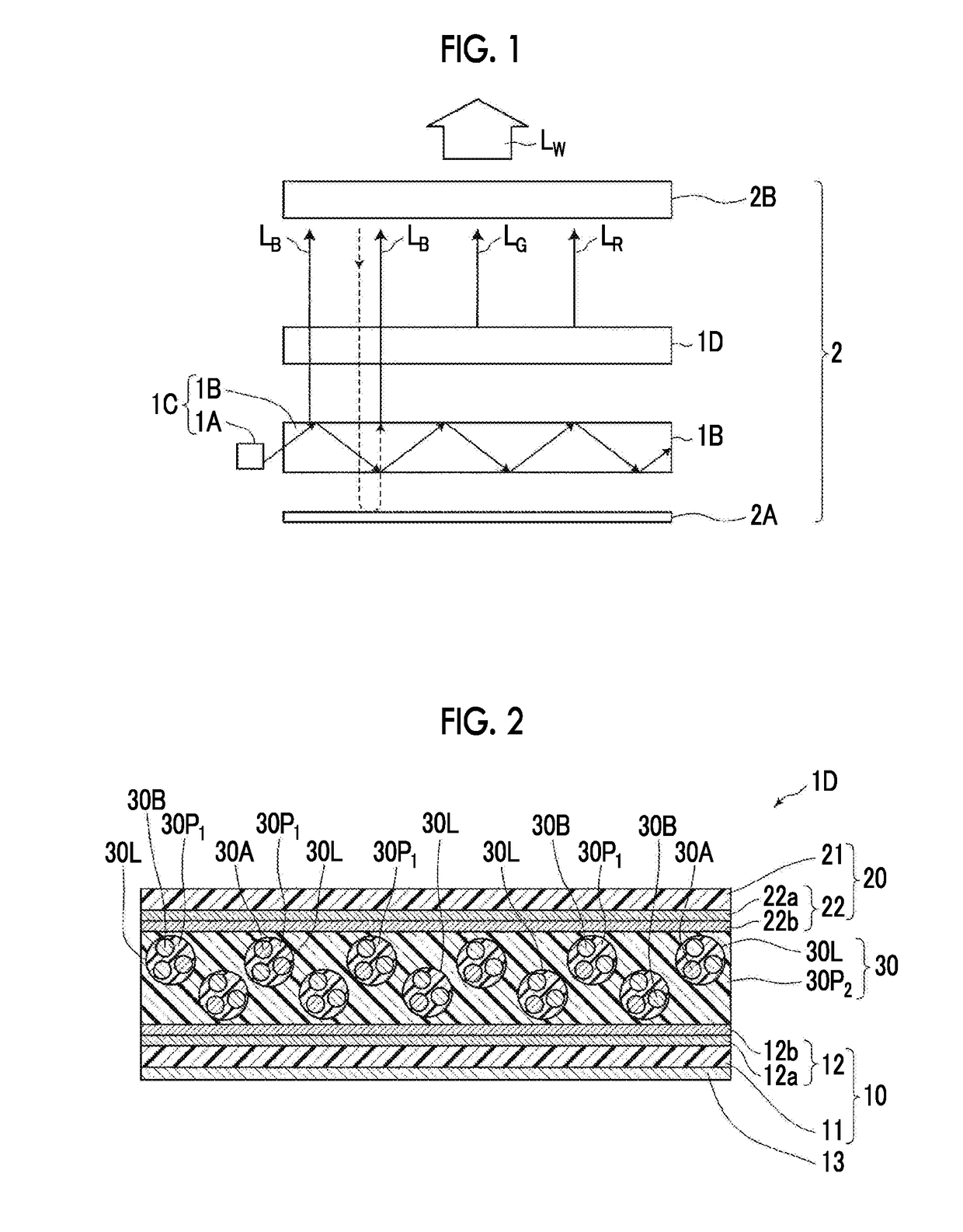
[0242](Preparation of Barrier Film 10)

[0243]As a support, a polyethylene terephthalate film (PET film; trade name: COSMOSHINE (registered trade name) A4300, manufactured by Toyobo Co., Ltd.) having a thickness of 50 μm was used, and an organic layer and an inorganic layer were formed in this order on a single surface of the support in the following procedure.

[0244]Trimethylolpropane triacrylate (TMPTA (trade name), manufactured by Daicel-Cytec Co., Ltd.) and a photopolymerization initiator (ESACURE KTO 46 (trade name), manufactured by Lamberti S.p.A.) were prepared and were weighed such th...


PUM

PropertyMeasurementUnit
sphericityaaaaaaaaaa
average particle diameteraaaaaaaaaa
wavelength rangeaaaaaaaaaa

Abstract

The invention provides a wavelength conversion member including a wavelength conversion layer which includes a second cured product and a first cured product dispersed as spheres in the second cured product, the first cured product being obtained by curing a first polymerizable composition including a quantum dot and a first polymerizable compound, and the second cured product being obtained by curing a second polymerizable composition including a second polymerizable compound. The invention further provides a backlight unit and a liquid crystal display device including the wavelength conversion member.

Description

CROSS-REFERENCE TO RELATED APPLICATIONS[0001]This application is a continuation application of International Application No. PCT / JP2015 / 006066, filed Dec. 7, 2015, which was published under PCT Article 21(2) in Japanese, the disclosure of which is incorporated herein by reference in its entirety. Further, this application claims priority from Japanese Patent Application No. 2014-249955, filed Dec. 10, 2014, the disclosure of which is incorporated herein by reference in its entirety.BACKGROUND OF THE INVENTION[0002]1. Field of the Invention[0003]The present invention relates to a wavelength conversion member, a backlight unit, a liquid crystal display device, and a method of manufacturing a wavelength conversion member.[0004]2. Description of the Related Art[0005]A flat panel display such as a liquid crystal display device (hereinafter also referred to as “LCD”) has been more widely used as a space-saving image display device having low power consumption. A liquid crystal display dev...

Claims


Application Information

Patent Timeline
Patent Type & Authority Applications(United States)
IPC IPC(8): G02F1/1335C09K11/56F21V8/00C09K11/02C08K9/10C09K11/88C08K3/30
CPCG02F1/133621C09K11/88C09K11/56C08K3/30G02F2001/133614C08K9/10G02B6/005C08K2201/011C08K2003/3036C09K11/02C09K11/08H01L33/50B29D11/00788C09K11/025C09K11/883G02F1/133614F21V9/30
Inventor YAMADA, NAOYOSHIITO, HIDEAKIHARA, TOSHIO
Owner FUJIFILM CORP
Why Eureka
Try Eureka