Semiconductor module and electric power conversion apparatus

a technology of semiconductor modules and electric power conversion apparatus, which is applied in the direction of electric variable regulation, process and machine control, instruments, etc., can solve the problems of difficult to significantly reduce the manufacturing cost of the entire semiconductor module is accordingly increased, and the surface area of the mosfet is large, so as to minimize the manufacturing cost of the entire semiconductor module and the effect of reducing the loss of the semiconductor modul

Active Publication Date: 2017-10-19
DENSO CORP
View PDF3 Cites 6 Cited by
  • Summary
  • Abstract
  • Description
  • Claims
  • Application Information

AI Technical Summary

Benefits of technology

[0007]With the above configuration, the surface area of the MOSFET is specified to be less than the surface area of the IGBT. Therefore, it is possible to minimize the surface area of the MOSFET that is made of the wide-bandgap semiconductor whose manufacturing cost is high. Consequently, it is possible to minimize the manufacturing cost of the entire semiconductor module.
[0008]Moreover, with the above configuration, in the low-current region, the electric current flows mainly through the MOSFET whose on-resistance is lower than the on-resistance of the IGBT in the low-current region. Consequently, it is possible to reduce the loss of the semiconductor module during its operation in the low-current region. In addition, since the MOSFET is mainly used in the low-current region, it is possible to minimize the surface area of the MOSFET as described above without making it difficult for the low electric current to flow mainly through the MOSFET.
[0009]Furthermore, with the above configuration, in the high-current region, the electric current flows mainly through the IGBT whose on-resistance is lower than the on-resistance of the MOSFET in the high-current region. Consequently, it is possible to reduce the loss of the semiconductor module during its operation in the high-current region. In addition, since the surface area of the IGBT is specified to be greater than the surface area of the MOSFET, it is possible to facilitate the flow of the high electric current mainly through the IGBT.
[0010]Accordingly, with the above configuration, in each of the low-current region and the high-current region, it is possible to have the electric current flow mainly through that one of the IGBT and the MOSFET whose on-resistance is lower than the other in the region. Consequently, it is possible to reduce the loss of the semiconductor module over the entire operating region.
[0011]To sum up, with the above configuration, it is possible to minimize the manufacturing cost of the semiconductor module and reduce the loss of the semiconductor module over the entire operating region.

Problems solved by technology

However, the manufacturing cost of a wide-bandgap semiconductor is high.
Therefore, increasing the chip area of the MOSFET, the manufacturing cost of the entire semiconductor module is accordingly increased.
Accordingly, in the high-current region, it is difficult to considerably reduce the loss of the semiconductor module by increasing the chip area of the MOSFET.

Method used


Image

  • Semiconductor module and electric power conversion apparatus
  • Semiconductor module and electric power conversion apparatus
  • Semiconductor module and electric power conversion apparatus

Examples


first embodiment

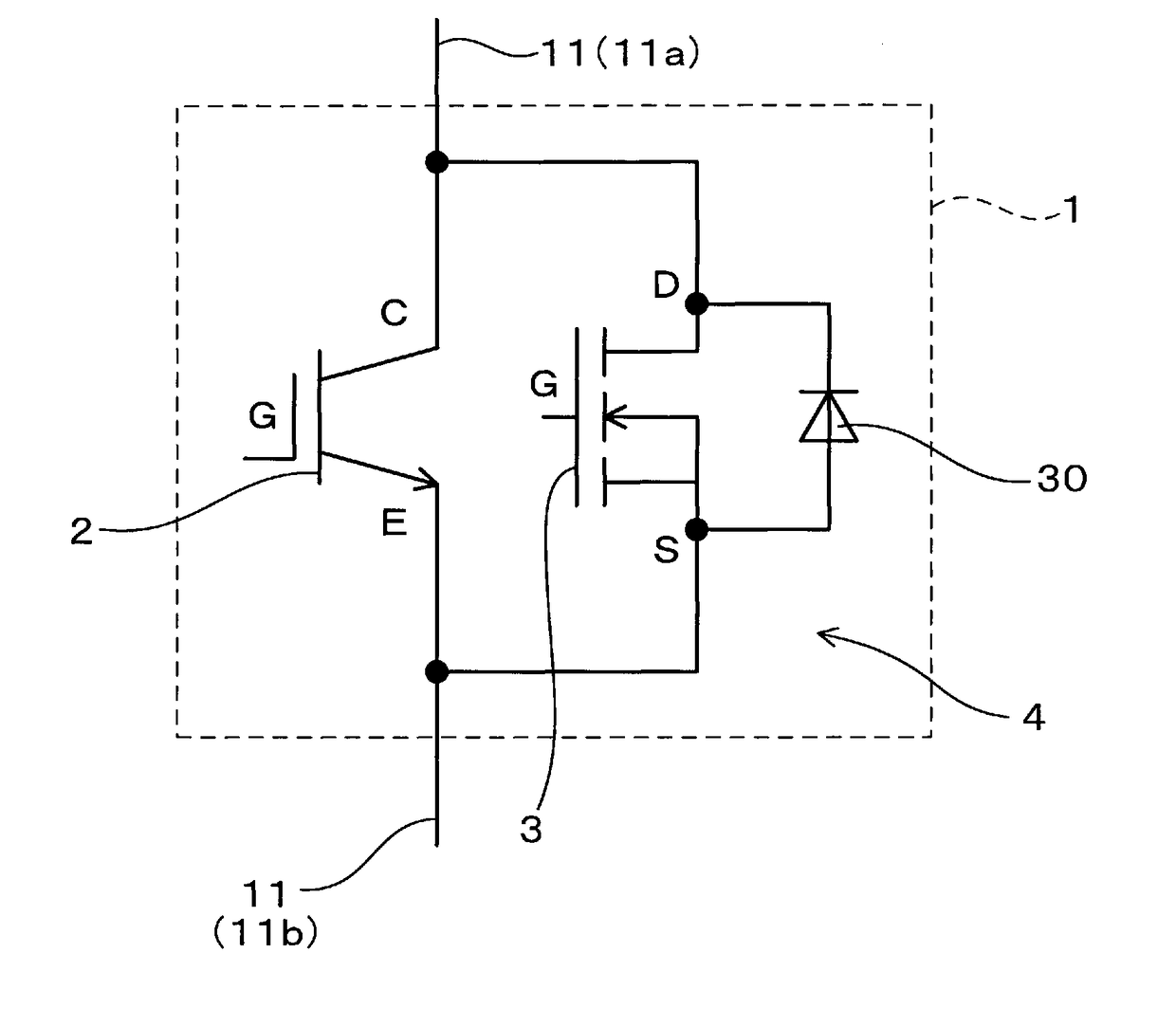
[0031]FIG. 1 shows the configuration of a semiconductor module 1 according to a first embodiment. As shown in the figure, the semiconductor module 1 includes an IGBT (Insulated-Gate Bipolar Transistor) 2 and a MOSFET (Metal-Oxide-Semiconductor Field-Effect Transistor) 3.

[0032]In the present embodiment, the IGBT 2 is made of a silicon semiconductor. The MOSFET 3 is made of a wide-bandgap semiconductor having a wider bandgap than the silicon semiconductor. More particularly, in the present embodiment, the MOSFET 3 is made of SiC.

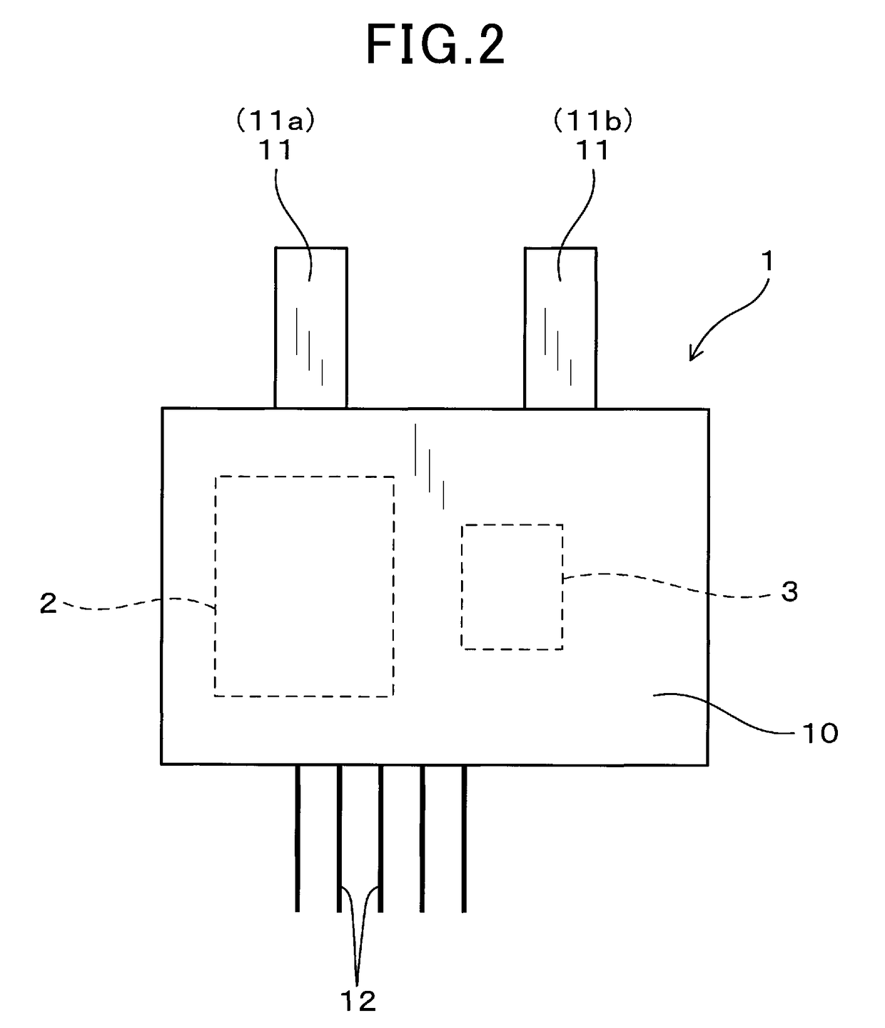
[0033]As shown in FIG. 1, in the present embodiment, the IGBT 2 and the MOSFET 3 are connected in parallel to each other to form a semiconductor element pair 4. Moreover, as shown in FIG. 2, the IGBT 2 has a greater surface area than the MOSFET 3.

[0034]As shown in FIG. 3, in the present embodiment, the semiconductor module 1 is configured to operate in a region which includes a low-current region AL and a high-current region AH. Electric current flowing throug...

second embodiment

[0060]FIG. 8 shows the configuration of a semiconductor module 1 according to a second embodiment.

[0061]Compared to the semiconductor modules 1 according to the first embodiment (see FIG. 1), the semiconductor module 1 according to the present embodiment further includes, as shown in FIG. 8, a diode 5 that is connected in antiparallel (or inverse parallel) to the MOSFET 3. The diode 5 is a Schottky barrier diode made of a wide-bandgap semiconductor such as SiC.

[0062]As shown in FIG. 9, in the present embodiment, the surface area SIGBT of the IGBT 2, the surface area SMOS of the MOSFET 3 and the surface area SDI of the diode 5 are set to satisfy the following relationship:

SIGBT>SMOS>SDI

[0063]Similar to the electric power conversion apparatus 6 according to the first embodiment (see FIG. 6), an electric power conversion apparatus 6 according to the present embodiment includes six semiconductor modules 1 (1H, 1L) according to the present embodiment. Moreover, three of the six semicond...

third embodiment

[0078]A semiconductor module 1 according to a third embodiment has almost the same configuration as the semiconductor modules 1 according to the second embodiment. Accordingly, the differences therebetween will be mainly described hereinafter.

[0079]In the second embodiment, the surface area SIGBT of the IGBT 2, the surface area SMOS of the MOSFET 3 and the surface area SDI of the diode 5 are set to satisfy the relationship of SIGBT>SMOS>SDI (see FIG. 9).

[0080]In comparison, in the present embodiment, as shown in FIG. 13, the surface area SIGBT of the IGBT 2, the surface area SMOS of the MOSFET 3 and the surface area SDI of the diode 5 are set to satisfy the following relationship:

SIGBT>SDI>SMOS

[0081]Moreover, in the present embodiment, the diode 5 is implemented by a Schottky barrier diode made of a wide-bandgap semiconductor (e.g., SiC) as in the second embodiment.

[0082]Similar to the electric power conversion apparatuses 6 according to the first and second embodiments (see FIG. 6...


PUM


Abstract

A semiconductor module includes an IGBT and a MOSFET. The IGBT is made of a silicon semiconductor. The MOSFET is made of a wide-bandgap semiconductor having a wider bandgap than the silicon semiconductor. The IGBT and the MOSFET are connected in parallel to each other to form a semiconductor element pair. The IGBT has a greater surface area than the MOSFET. The semiconductor module is configured to operate in a region that includes a low-current region and a high-current region. Electric current flowing through the semiconductor element pair is higher in the high-current region than in the low-current region. In the low-current region, the on-resistance of the MOSFET is lower than the on-resistance of the IGBT. In contrast, in the high-current region, the on-resistance of the IGBT is lower than the on-resistance of the MOSFET.

Description

CROSS-REFERENCE TO RELATED APPLICATION[0001]This application is based on and claims priority from Japanese Patent Application No. 2016-84052 filed on Apr. 19, 2016, the content of which is hereby incorporated by reference in its entirety into this application.BACKGROUND1 Technical Field[0002]The present invention relates to semiconductor modules that have semiconductor elements built therein and electric power conversion apparatuses that employ the semiconductor modules.2 Description of Related Art[0003]There are known semiconductor modules that are employed in electric power conversion apparatuses (see, for example, Japanese Patent Application Publication No. JP2014229642A). The semiconductor modules have, for example, an IGBT (Insulated-Gate Bipolar Transistor) built therein; the IGBT is made of a silicon semiconductor. The electric power conversion apparatuses are configured to perform electric power conversion by controlling switching of the IGBT.[0004]In recent years, there has...

Claims


Application Information

Patent Timeline
Patent Type & Authority Applications(United States)
IPC IPC(8): H02M3/158H01L29/20H01L25/07H01L29/16H01L29/861H01L29/739
CPCH02M3/158H01L29/2003H01L29/7393H01L25/07H01L29/861H01L29/1608H01L27/0203H01L27/0207H02M1/00H02M1/08H02M1/088H02M7/5387H01L25/072H01L25/18
Inventor SHIMIZU, HIROSHIKIMURA, MITSUNORIMOCHIKI, KENGOYAMAHIRA, YUUMATSUOKA, TETSUYAFUKUSHIMA, KAZUMAOHKOUCHI, YASUYUKI
Owner DENSO CORP
Why Eureka
Try Eureka