Semiconductor device for detecting ultraviolet and infrared radiation and related manufacturing process

a semiconductor and infrared radiation technology, applied in the direction of optical radiation measurement, instruments, lighting and heating apparatus, etc., can solve the problems of generating false alarms, high cost of gas photomultiplier tubes, and large overall dimensions,

Active Publication Date: 2017-11-02
STMICROELECTRONICS SRL
View PDF2 Cites 41 Cited by
  • Summary
  • Abstract
  • Description
  • Claims
  • Application Information

AI Technical Summary

Benefits of technology

[0010]According to one or more embodiments of the disclosure, a semiconductor device for flame detection includes:

Problems solved by technology

However, gas photomultiplier tubes have high costs and large overall dimensions.
Furthermore, the use of ultraviolet sensors is limited to indoor and short-range applications since ultraviolet radiation undergoes a high attenuation in the presence, for example, of dust, smoke, hydrocarbon vapours, etc.
However, they may generate false alarms owing to emission of infrared radiation by sources that are not dangerous (for example, matches), or else to emission of black-body radiation by objects at high temperature (for example, hot metal objects).
Flame sensors of a combined type are characterized in any case by large overall dimensions, as well as by high costs.
Furthermore, prior art flame sensors of a combined type require generation of high voltages in order to drive the gas photomultiplier tubes, and have a low sensitivity in the infrared, since pyroelectric sensors have a low sensitivity.

Method used


Image

  • Semiconductor device for detecting ultraviolet and infrared radiation and related manufacturing process
  • Semiconductor device for detecting ultraviolet and infrared radiation and related manufacturing process
  • Semiconductor device for detecting ultraviolet and infrared radiation and related manufacturing process

Examples


Embodiment Construction

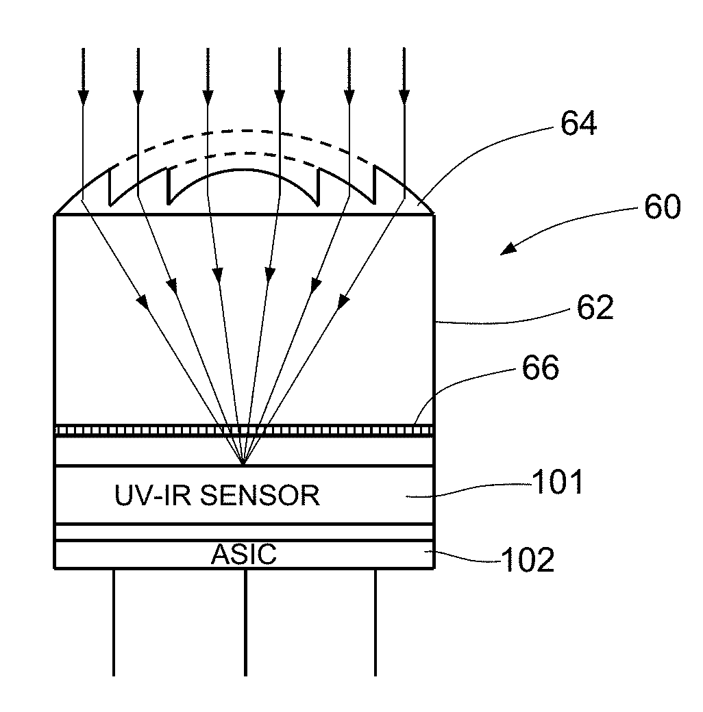
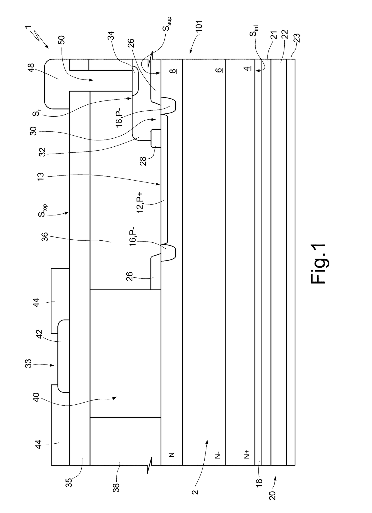
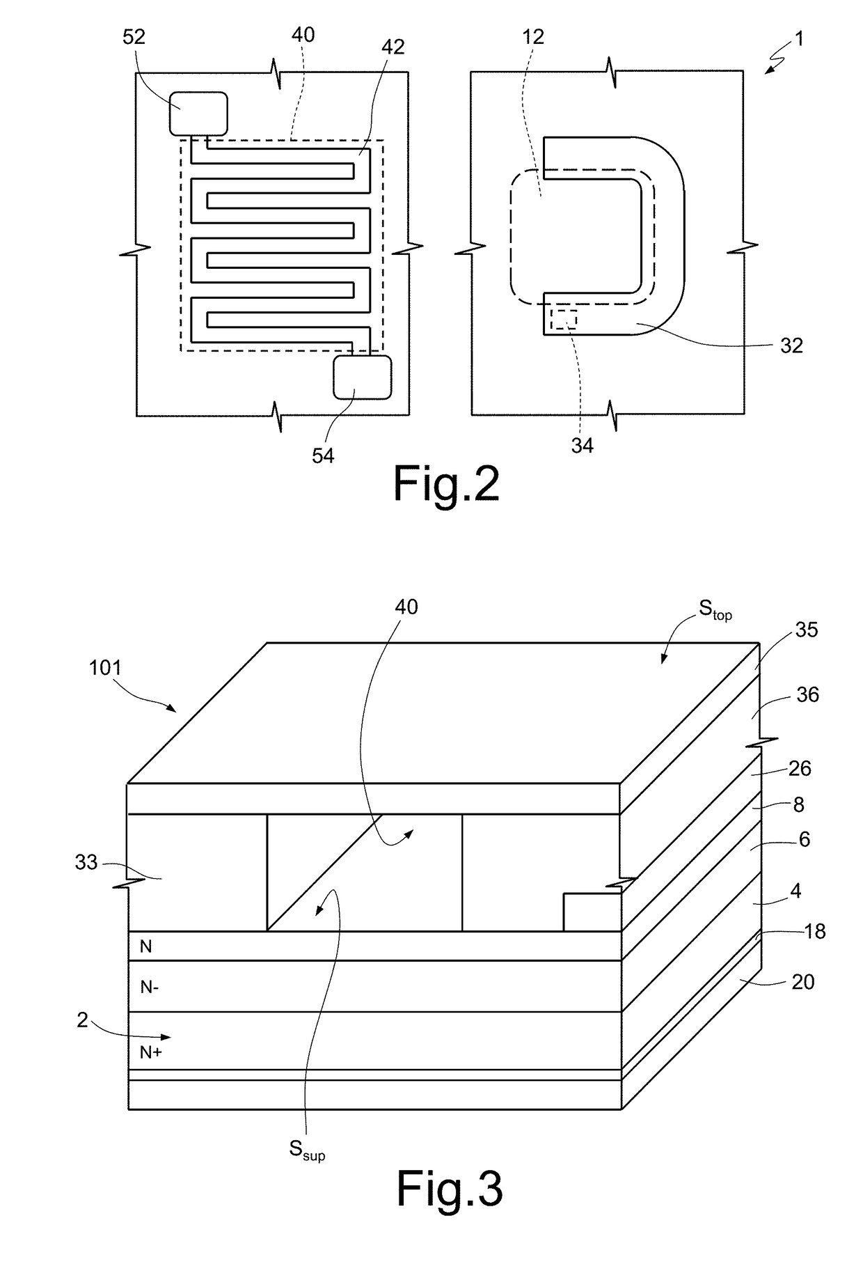
[0027]FIG. 1 shows an example of embodiment of a semiconductor device 1, which is integrated in a first die 101. FIG. 1 and the subsequent figures are not in scale.

[0028]In detail, the semiconductor device 1 comprises a semiconductor body 2, for example of silicon carbide. In particular, the semiconductor body 2 may be made of silicon carbide of a 4H polytype (4H—SiC).

[0029]The semiconductor body 2 includes a substrate 4 of an N+ type, which is delimited at the bottom by a bottom surface Sinf, and has a thickness, for example, of 350 μm; moreover, the substrate 4 is doped, for example, with nitrogen and has a doping level of, for example, 1·1019 cm−3. Without any loss of generality, in what follows it is assumed, wherever not expressly indicated, that the doping of an N type is obtained using nitrogen as dopant.

[0030]The semiconductor body 2 further comprises a first epitaxial layer 6 and a second epitaxial layer 8.

[0031]The first epitaxial layer 6 is arranged on the substrate 4, is...


PUM


Abstract

A semiconductor device for flame detection, including: a semiconductor body having a first conductivity type conductivity, delimited by a front surface and forming a cathode region; an anode region having a second conductivity type conductivity, which extends within the semiconductor body, starting from the front surface, and forms, together with the cathode region, the junction of a photodiode that detect ultraviolet radiation emitted by the flames; a supporting dielectric region; and a sensitive region, which is arranged on the supporting dielectric region and varies its own resistance as a function of the infrared radiation emitted by the flames.

Description

BACKGROUNDTechnical Field[0001]The present disclosure relates to a semiconductor device for detecting ultraviolet and infrared radiation; moreover, the present disclosure relates to the process for manufacturing this semiconductor device.Description of the Related Art[0002]As is known, so-called flame sensors are today available, which are devices designed to detect the presence of flames. These sensors are commonly used both in the industrial field (for example, in order to verify that a furnace plant is operating properly), and in the domestic field (for example, in order to detect possible gas leaks accompanied by explosions).[0003]The flames that are generated following upon combustion of hydrocarbons are accompanied by simultaneous emission of electromagnetic radiation in the ultraviolet spectral region, i.e., radiation with wavelengths comprised between 100 nm and 400 nm, as well as in the infrared spectral region, i.e., radiation with wavelengths comprised between 700 nm and ...

Claims


Application Information

Patent Timeline
Patent Type & Authority Applications(United States)
IPC IPC(8): G01J1/42H01L31/107H01L31/0352H01L31/0312H01L31/0232H01L31/0224H01L31/0216H01L31/02G01J5/00H01L31/18F23N5/08
CPCG01J1/429H01L31/022408H01L31/107H01L31/0312H01L31/035281G01J5/0014H01L31/02327H01L31/02027H01L31/1812F23N5/082H01L31/02164G01J5/20H01L27/14609H01L27/14625H01L27/14669H01L27/1467H01L31/022416G01J1/0488G01J2001/0496G01J1/0411G01J1/0209H01L31/1035H01L31/09H01L31/103
Inventor MAZZILLO, MASSIMO CATALDOSCIUTO, ANTONELLA
Owner STMICROELECTRONICS SRL
Why Eureka
Try Eureka