Electret element and manufacturing method therefor, sensor, electronic circuit, and input device

a manufacturing method and technology of a semiconductor element, applied in the direction of acceleration measurement using interia force, pulse technique, instruments, etc., can solve the problems of inability to detect applied pressure, complicated manufacturing process, and inability to improve the yield of the product, so as to achieve high surface potential, high surface potential, and high surface potential.

Active Publication Date: 2017-11-16
CONTINUOUS COMPOSITES INC +1
View PDF5 Cites 3 Cited by
  • Summary
  • Abstract
  • Description
  • Claims
  • Application Information

AI Technical Summary

Benefits of technology

[0020]A novel structure and operational mechanism using the electret film and the semiconductor allow achieving a simply structured, high-precision thin-film element for detecting pressure.
[0021]According to the electret element of the present invention, since a gap between an electret surface, which has a high surface potential, and a semiconductor surface varies depending on applied pressure at a pressing time, and the applied pressure can be detected by utilizing a correlation between variance of the gap and conductivity of a conductive channel formed in the semiconductor. This enables highly sensitive pressure detection.
[0022]According to the electret element of the present invention, the conductivity of the conductive channel formed in the semiconductor contacting with the electret surface, which has a high surface potential, varies depending on the applied pressure at the pressing time etc., and the applied pressure can be detected by utilizing this variance. This enables highly sensitive pressure detection.
[0023]The electret element of the present invention makes it possible to increase in high sensitivity and high precision of a touch input device for an electronic device such as a touch panel. Also, the electret element of the present invention can be utilized in such a device as a pressure sensing sheet, a vibration detecting sensor, and a sound sensing microphone. Further, if a structure of the electret element is made of a flexible material(s), a thin-film flexible sensor device and a flexible input device having them as an input terminal(s) can be achieved.
[0024]Particularly, according to the electret element of the present invention, since an electric signal responds sensitively to a minute vertical displacement of the electret film, extremely weak touches by a pen, a brush, or the like, which is a difficult operation for a conventional touch panel to carry out, can be clearly distinguished. The element for a touch sensor with high precision and high sensitivity can be thus achieved.

Problems solved by technology

Also, the capacitance type touch sensor used in a conventional touch panel etc. can detect the location information, but has a problem of enabling no detection of applied pressure.
Meanwhile, the in-cell type touch panel etc., in which the touch sensor is incorporated in the display element, have a problem of making a manufacturing process complicated, and making its yield not improved.
Further, there is also another problem of bringing an increase in manufacturing cost due to much use of a vacuum process, and a lithographic process, etc.

Method used


Image

  • Electret element and manufacturing method therefor, sensor, electronic circuit, and input device
  • Electret element and manufacturing method therefor, sensor, electronic circuit, and input device
  • Electret element and manufacturing method therefor, sensor, electronic circuit, and input device

Examples


first embodiment

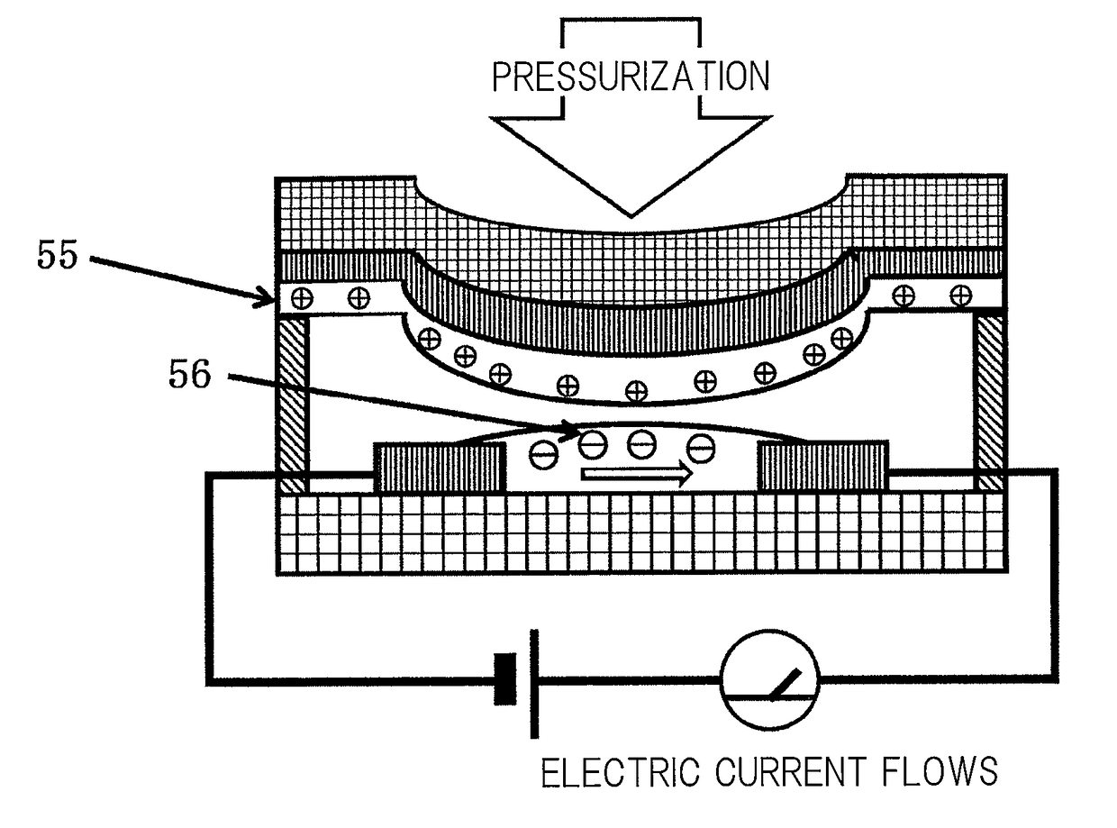
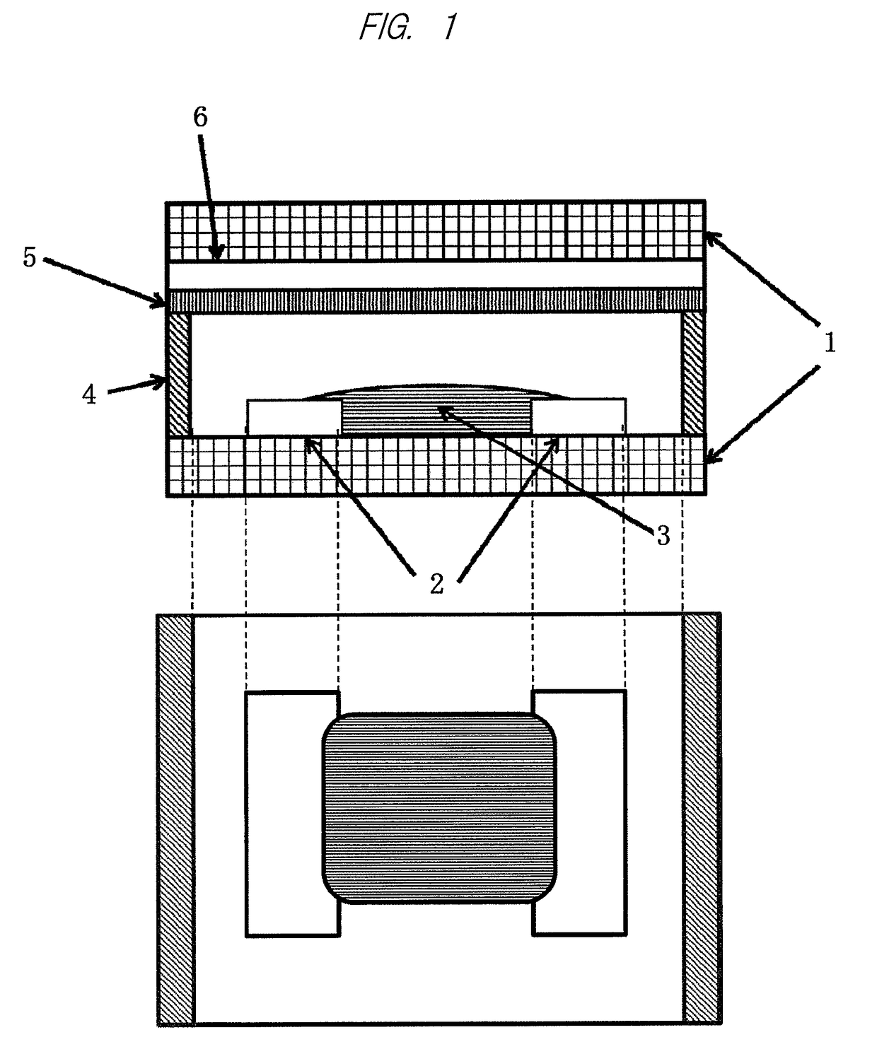
[0056]A first embodiment will hereinafter be described in reference to the drawings. FIG. 1 is a conceptual diagram of an electret element of the first embodiment, in which its upper side is a sectional view and its lower side is a plan view corresponding to the sectional view. The present element has a basic structure including: a pair of electrodes 2; a semiconductor 3 sandwiched between the pair of electrodes 2; and an electret film 5 disposed at a location opposite to the semiconductor 3 via a gap so as to oppose a surface of the semiconductor. According to this embodiment, the pair of electrodes 2 and the semiconductor 3 are mounted on the lower substrate 1 on the upper side of the Figure, and a bank structure body 4 serving as a structure for providing the gap is provided at least at a circumference of the semiconductor and outside each periphery of the paired electrodes 2. The bank structure body 4 is provided on a part or the whole of an outer periphery of the electret film ...

second embodiment

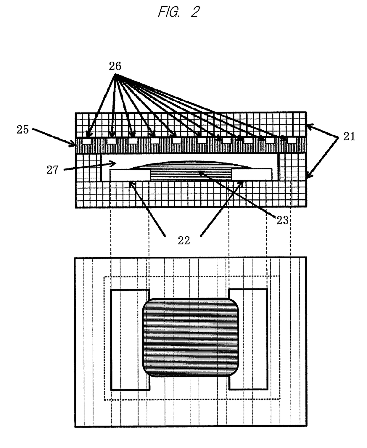
[0068]A second embodiment will hereinafter be described in reference to the drawings. According to the present embodiment, a plurality of the electret elements described in the first embodiment are provided, and presence / absence or magnitude of pressure or vibration applied to the electret film are detected through an electric current flowing between the pair of electrodes, so that a position of the detection is detected. A device of the present embodiment is suitable to an input device used in an electronic device such as a touch panel. FIG. 9 illustrates a schematically plan view of the device of the present embodiment seen from above. FIG. 9 is an example in which a plurality of the electret elements are arranged in a first direction and a second direction crossing the first direction (for example, at right angles) to form an array of the elements. FIG. 9 shows an example of an 8×8 matrix array circuit. Rows of independent wirings are provided in the first and second directions, ...

third embodiment

[0069]According to a third embodiment, the gap holding portion such as the bank structure body on the electret element of the first embodiment is removed, and the semiconductor and the electret film make up a stack structure. The third embodiment will hereinafter be described in reference to the drawings. FIG. 10 is a conceptual diagram of an electret element of the present embodiment, in which its upper side is a sectional view and its lower side is a plan view corresponding to the sectional view.

[0070]An amount of electric charges induced in the semiconductor varies depending not only on a distance between the semiconductor and the electret film but also on a difference in force with which the electret film presses a semiconductor layer. Therefore, the amount of electric current flowing through the semiconductor lying between the electrodes can be controlled by changing the pressure applied to the electret film in such a state that the electret film contacts with the semiconductor...


PUM


Abstract

Provided are an element applicable to a high-precision, high-sensitivity pressure detecting sensor and switch, a manufacturing method for the element; and a sensor, an electronic circuit, and an input device that include the element. The electret element of the present invention has a semiconductor sandwiched between a pair of electrodes, and an electret film disposed at a location opposite to the semiconductor via a gap. The electret element of the present invention may be structured so that the semiconductor contacts with the electret film, or so as to have micro-sized gaps therebetween. The electret film is semi-permanently kept in a positively or negatively charged state. By having a structure in which the electret film can contact with or approach the semiconductor, an amount of electric currents flowing between the pair of electrodes can be controlled.

Description

CROSS-REFERENCE TO RELATED APPLICATIONS[0001]This application is a National Stage application of International Patent Application No. PCT / JP2015 / 077558, filed on Sep. 29, 2015, which claims priority to Japanese Patent Application Number 2014-204038, filed on Oct. 2, 2014, each of which is hereby incorporated by reference in its entirety.TECHNICAL FIELD[0002]The present invention relates to: an electret element applicable to a high-precision, high-sensitivity pressure detecting sensor and switch; a manufacturing method for the electret element; and a sensor, an electronic circuit, and an input device each of which has the electret element.BACKGROUND ART[0003]Development of an input device such as a touch sensor has been in progress in recent years. For example, a capacitance type touch sensor is used in a touch panel etc., thereby enabling detection of input location information. An in-cell type touch panel, in whose display element a touch sensor is incorporated, and the like are al...

Claims


Application Information

Patent Timeline
Patent Type & Authority Applications(United States)
IPC IPC(8): G06F3/041H01L29/84H01L29/82G06F3/01H01L29/51H01L21/31G01P15/08G06F3/0354H01L41/113H01L29/78
CPCG06F3/041G06F3/016G06F3/03545H01L21/31H01L29/513H01L29/78H01L29/82H01L29/84H01L41/1132G01P15/08B81B2201/0264B81B2201/0257H01G7/02H03K17/955H03K17/975B81B3/0021G01L1/2293G06F3/04146G06F3/044H10N30/302
Inventor KOZASA, TAKEHITOYOSHIDA, MANABU
Owner CONTINUOUS COMPOSITES INC
Why Eureka
Try Eureka