Glass sheet

Active Publication Date: 2017-11-23
NIPPON ELECTRIC GLASS CO LTD
View PDF2 Cites 3 Cited by
  • Summary
  • Abstract
  • Description
  • Claims
  • Application Information

AI Technical Summary

Benefits of technology

[0007]In order to suppress a change in dimension of a substrate to be processed, it is effective to use a glass sheet as a supporting sheet. The glass sheet is smoothened easily on the surface thereof and has stiffness. Accordingly, when the glass sheet is used, the substrate to toe processed can be supported strongly and accurately. In addition, the glass sheet easily tra

Problems solved by technology

Alone with this, a mounting space for semiconductor chips to be used in those electronic devices is strictly limited, and there is a problem of high-density mounting of the semiconductor chips.
However, the conventional WLP has problems in that it is difficult to increase the number of pins, and chipping and the like of semiconductor chips are liable to occur because the semiconductor chips are mounted in a state in which the back surfaces th

Method used


Image

  • Glass sheet
  • Glass sheet
  • Glass sheet

Examples


example 1

[0089]Now, the present invention is described with reference to Examples. However, Examples below are merely examples, and the present invention is by no means limited to the following Examples.

[0090]Glass raw materials were blended so as to comprise as a glass composition, in terms of mass %, 65.5% of SiO2, 8% of Al2O3, 9% of B2O3, 13.1% of Na2O, 3% of CaO, 1% of ZnO, 0.3% of SnO2, and 0.1% of Sb2O3. After that, the resultant was loaded into a glass melting furnace to be melted at from 1,500° C. to 1,600° C. Then, the molten glass, was supplied into an overflow down-draw forming apparatus to be formed to a thickness of 1.0 mm. Further, the resultant was cut to a predetermined size and subjected to annealing treatment.

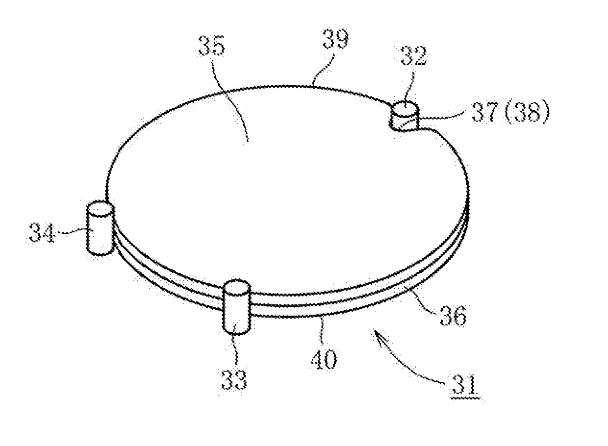
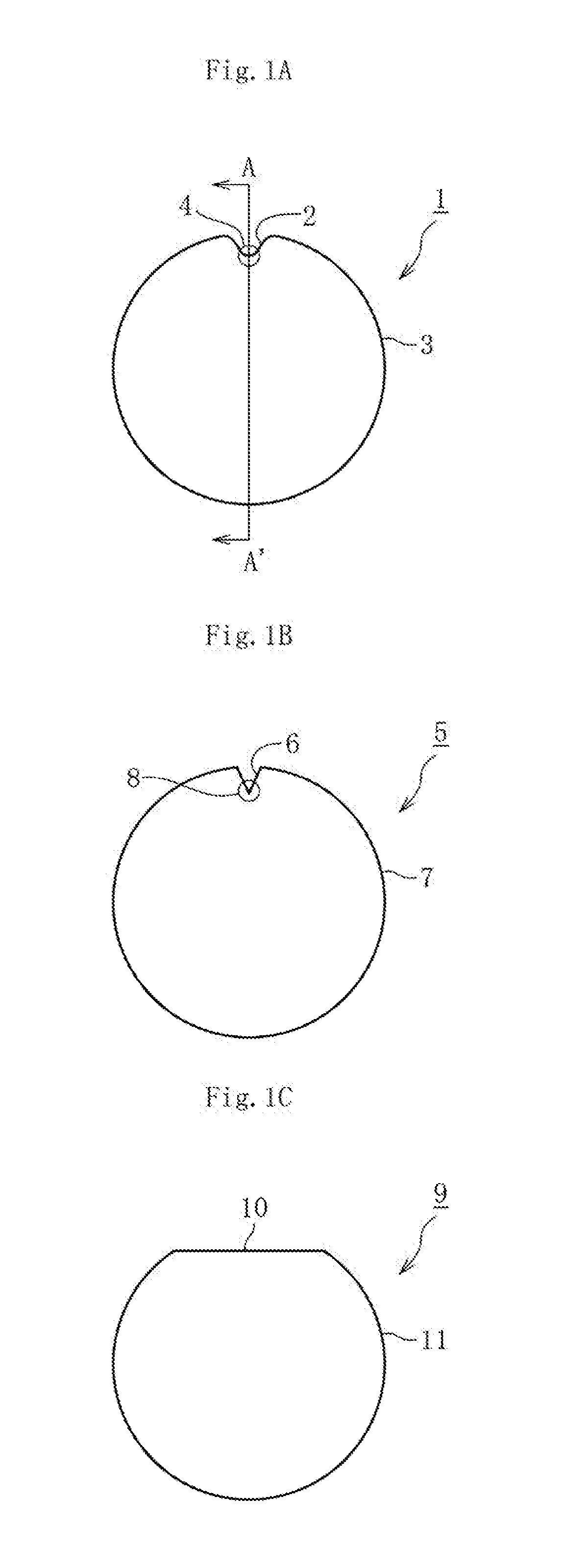
[0091]Next, the outer periphery of the obtained glass sheet was processed into a perfectly circular shape of σ 300 mm. After that, a semicircular recess, that is, a position alignment portion having a notch shape (depth: 1.1 mm) was formed, and the position alignment p...

example 2

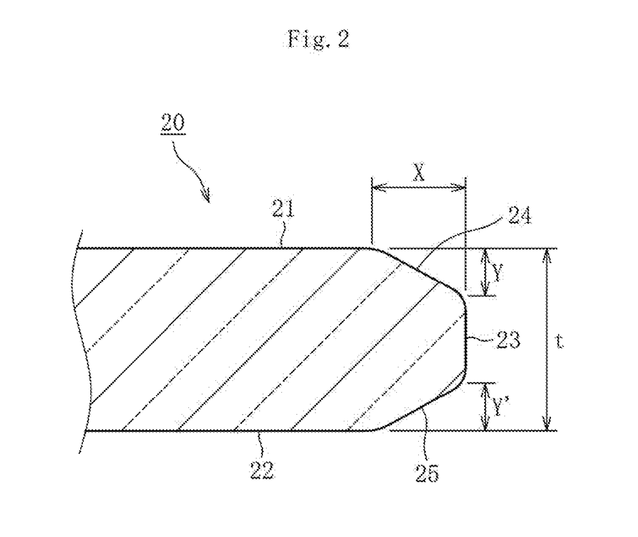
[0095]First, glass raw materials were blended so as to have a glass composition of each of Sample Nos. 1 to 7 shown in Table 2. After that, the resultant was loaded into a glass melting furnace to be melted at from 1,500° C. to 1,600° C. Then, the molten glass was supplied into an overflow down-draw forming apparatus to be formed to a thickness of 0.8 mm. After that, in the same manner as in [Example 1], outer periphery processing was performed, and a position alignment portion having a semicircular recess was formed. Next, the position alignment portion and the contour portion were subjected to chamfering processing. In the chamfering processing, a chamfer width in a thickness direction was set to 50% of a thickness, and a chamfer width in a surface direction was set to 600 μm. In addition, a boundary between the position alignment portion and the contour portion of the glass sheet was processed into a continuously rounded state. Polishing pads used in the chamfering processing are...

example 3

[0103]For each of the position alignment portion and the region except for the position alignment portion (contour portion) of the glass sheet according to Sample No. 2 obtained in [Example 1], the entire end surface including the chamfered surface was subjected to mirror surface polishing treatment, and then the surface of the glass sheet was subjected to polishing treatment with a polishing apparatus by the same method as that of [Example-1]. Polishing pads used in the mirror surface polishing treatment are made of urethane, and the surface subjected to the mirror surface polishing treatment has a polishing roughness of #3000. For comparison, there was also produced a glass sheet in which the entire end surface including the chamfered surface was subjected to polishing treatment with #1500 polishing pads.

[0104]Subsequently, for each of the obtained glass sheets, the surface roughness of the end surface including the chamfered surface was measured by a method in accordance with JIS...


PUM

PropertyMeasurementUnit
Fractionaaaaaaaaaa
Fractionaaaaaaaaaa
Thicknessaaaaaaaaaa

Abstract

A technical object of the present invention is to devise a glass sheet that facilitates position alignment with a substrate to be processed and is less liable to be broken during conveyance, or processing treatment of the substrate to be processed, to thereby contribute to an increase in density of a semiconductor package. In order to achieve the technical object, the glass sheet of the present invention includes, in a contour thereof: a contour portion; and a position alignment portion, in which all or part of an end edge region of the position alignment portion where a surface thereof and an end surface thereof intersect is chamfered.

Description

TECHNICAL FIELD[0001]The present invention relates to a glass sheet, and more specifically, to a glass sheet to be used for supporting a substrate to fee processed in a manufacturing process for a semiconductor package.BACKGROUND ART[0002]Portable electronic devices, such as a cellular phone, a notebook-size personal computer, and a personal data assistance (PDA), are required to be downsized and reduced in weight. Alone with this, a mounting space for semiconductor chips to be used in those electronic devices is strictly limited, and there is a problem of high-density mounting of the semiconductor chips. In view of this, in recent years, there has been an attempt to perform high-density mounting of a semiconductor package by a three-dimensional mounting technology, that is, by laminating semiconductor chips on top of another and connecting the semiconductor chips through wiring,[0003]In addition, a conventional wafer level package (WLP) is manufactured by forming bumps into a wafer...

Claims


Application Information

Patent Timeline
IPC IPC(8): C03C19/00H01L23/00C03B17/06
CPCC03C19/00H01L2224/95001C03B17/064H01L24/96B32B7/06B32B7/12B32B17/06C03C3/091C03C3/093H01L23/3128H01L21/561H01L21/568H01L21/6835H01L2221/68318H01L2224/04105H01L2224/12105H01L2224/96H01L2224/11H01L2224/03B32B17/00H01L23/15Y02P40/57B32B2457/14Y02P40/50
Inventor KATAYAMA, HIROKINAKAJIMA
Owner NIPPON ELECTRIC GLASS CO LTD
Why Eureka
Try Eureka