Apparatus with 3D wirewound inductor integrated within a substrate

a technology of inductor and substrate, applied in the field of inductor, can solve the problems of processing used to form vias and traces, and incur fabrication costs, and achieve the effects of reducing the number of metal traces of the device, increasing the circuit area density of the device, and enhancing device performan

Inactive Publication Date: 2017-11-23
QUALCOMM INC
View PDF1 Cites 17 Cited by
  • Summary
  • Abstract
  • Description
  • Claims
  • Application Information

AI Technical Summary

Benefits of technology

[0006]By integrating the one or more 3D wirewound inductors within the substrate, a number of metal traces of the device may be reduced as compared to a device that uses vias and traces to form an inductor. As a result, certain device components may be formed on (or “stacked” on) an inductor, increasing circuit area density of the device. For example, an inductive-capacitive (LC) filter may include a 3D wirewound inductor integrated within a substrate and may

Problems solved by technology

Further, processes used to form the v

Method used


Image

  • Apparatus with 3D wirewound inductor integrated within a substrate
  • Apparatus with 3D wirewound inductor integrated within a substrate
  • Apparatus with 3D wirewound inductor integrated within a substrate

Examples


Embodiment Construction

[0021]Certain examples are described below with reference to the drawings. In the description and the drawings, similar or common features are indicated by common reference numbers.

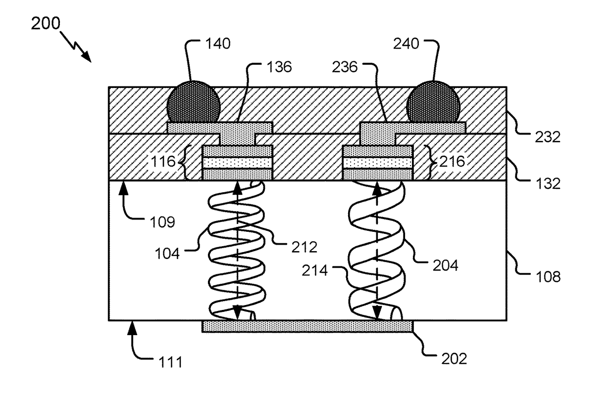
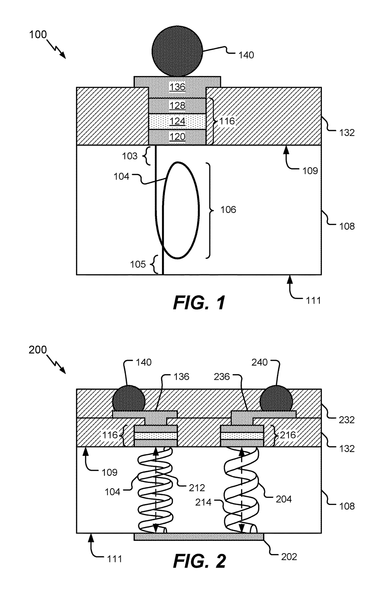
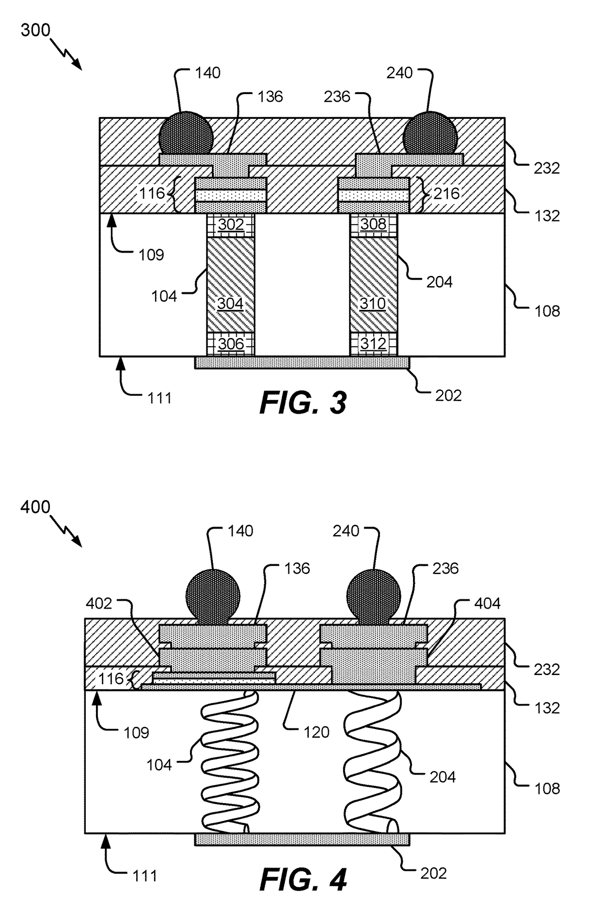
[0022]FIG. 1 depicts an illustrative example of a device 100, such as an integrated circuit (IC) or a hybrid integrated circuit (HIC). The device 100 includes a three-dimensional (3D) wirewound inductor 104 disposed within (e.g., embedded within) a substrate 108. The device 100 may have a passive-on-glass (PoG) configuration.

[0023]The 3D wirewound inductor 104 may have a monolithic configuration and may be formed from a single material (e.g., instead of using vias and traces that are formed in multiple steps of lithography and metal deposition). The 3D wirewound inductor 104 may include a metal material, such as copper or tungsten, as illustrative examples.

[0024]The 3D wirewound inductor 104 includes one or more coils, such as a coil 106. The coil 106 may be disposed between a first surface 109 of the sub...


PUM


Abstract

An apparatus includes a substrate and a three-dimensional (3D) wirewound inductor integrated within the substrate. The apparatus further includes a capacitor coupled to the 3D wirewound inductor.

Description

I. FIELD[0001]This disclosure is generally related to electronic devices and more particularly to inductors.II. DESCRIPTION OF RELATED ART[0002]Integrated circuits and other electronic devices may include inductors, capacitors, and other components. An inductor may generate a magnetic field in response to a current.[0003]Certain integrated circuits and other devices include inductors formed using vias. For example, metal vias may be formed in a substrate, and the metal vias may be connected using a trace. The metal vias and the trace may form a “U” shape that functions as an inductor by generating a magnetic field in response to a current.[0004]Inductors formed using vias and traces utilize circuit area of an integrated circuit. For example, surface area of an integrated circuit may be used to form the traces that connect the vias. The traces reduce surface area of the integrated circuit available to other device components of the integrated circuit. Further, processes used to form ...

Claims


Application Information

Patent Timeline
IPC IPC(8): H01F27/40H01F41/02H01F27/28H01F27/29H03H7/46H03H7/01
CPCH01F27/40H01F27/2823H03H7/466H01F41/02H03H7/0115H01F27/29H01F17/00H01L23/5227H01L23/49822H01L23/5223H01L28/10H01F27/292H01F2017/002
Inventor YUN, CHANGHAN HOBIEZUO, CHENGJIEKIM, DAEIK DANIELVELEZ, MARIO FRANCISCOMUDAKATTE, NIRANJAN SUNILKIM, JONGHAEBERDY, DAVID FRANCIS
Owner QUALCOMM INC
Why Eureka
Try Eureka