Display device

a display device and display technology, applied in semiconductor devices, instruments, electrical equipment, etc., can solve the problems of low carrier mobility of taos, difficult to form drive circuits to be installed, and inability to use the same process for taos, so as to reduce leak current, keep down leak current, and low carrier mobility

Active Publication Date: 2017-11-23
JAPAN DISPLAY INC
View PDF3 Cites 17 Cited by
  • Summary
  • Abstract
  • Description
  • Claims
  • Application Information

AI Technical Summary

Benefits of technology

[0006]The TFT used for the switching of a pixel is required to keep down its leak current. The use of an oxide semiconductor for the TFT can reduce the leak current. In the following description, a type of oxide semiconductor that is optically transparent and not crystalline will be referred to as TAOS (transparent amorphous oxide semiconductor). Examples of TAOS include indium gallium zinc oxide (IGZO), indium tin zinc oxide (ITZO), zinc oxide nitride (ZnON), indium gallium oxide (IGO), and so forth. However, TAOS has low carrier mobility, and thus there are cases where it is difficult to form a drive circuit to be installed in a display device with TFTs using TAOS. The term “TAOS” will hereinafter be used also in the meaning of a TFT using TAOS.

Problems solved by technology

However, TAOS has low carrier mobility, and thus there are cases where it is difficult to form a drive circuit to be installed in a display device with TFTs using TAOS.
However, in cases where LTPS is used for a switching TFT in a pixel, two LTPSs are usually used in series connection since LTPS has high leak current.
However, LTPS and TAOS have material characteristics different from each other and there is a problem in forming them on the same substrate.
However, it is impossible to use the same process for TAOS since TAOS is dissolved by hydrofluoric acid (HF).

Method used


Image

  • Display device
  • Display device
  • Display device

Examples


first embodiment

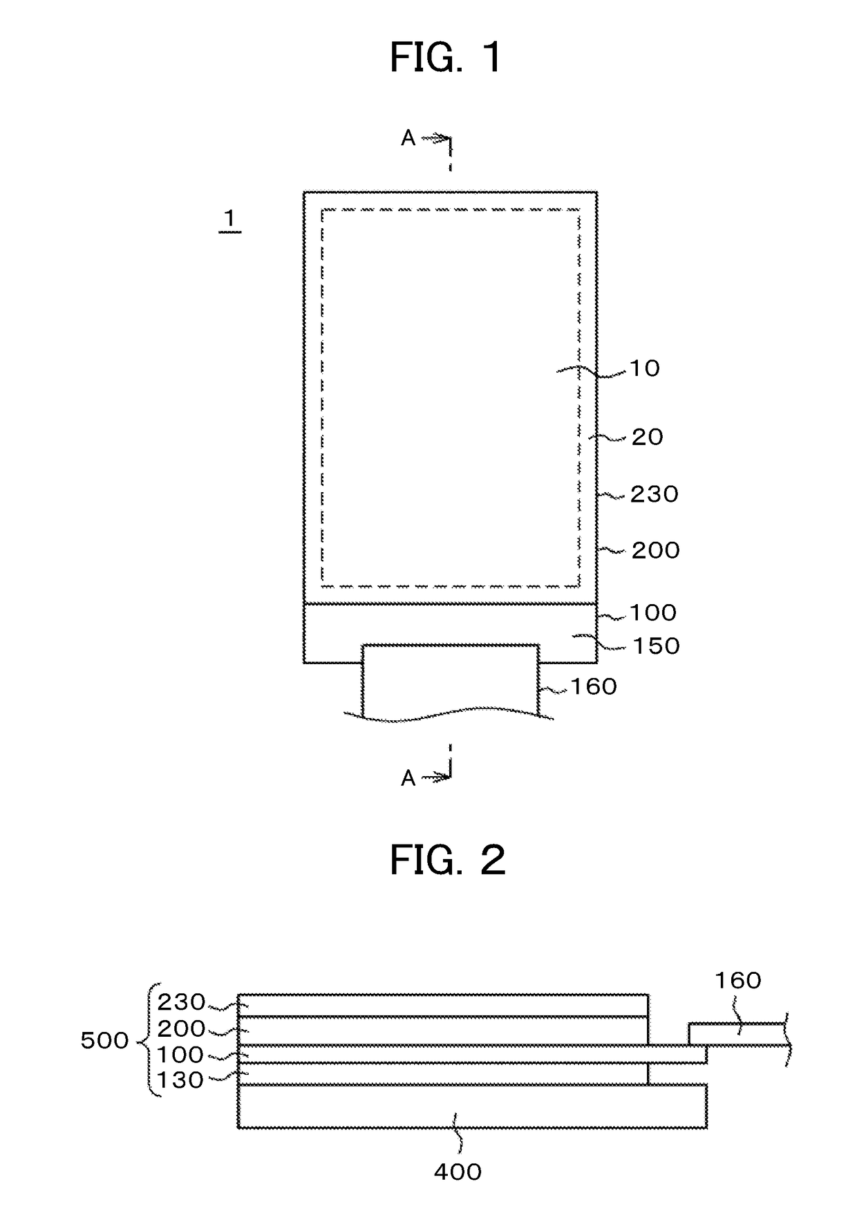
[0038]FIG. 1 is a plan view of a liquid crystal display device 1 to which the present invention is applied. FIG. 2 is a cross-sectional view taken along the line A-A in FIG. 1. In FIGS. 1 and 2, a TFT substrate 100 and a counter substrate 200 are formed to face each other and a liquid crystal is sandwiched between the TFT substrate 100 and the counter substrate 200. A lower polarizing plate 130 is bonded to a lower surface of the TFT substrate 100, while an upper polarizing plate 230 is bonded to an upper surface of the counter substrate 200. The combination of the TFT substrate 100, the counter substrate 200, the lower polarizing plate 130 and the upper polarizing plate 230 will be referred to as a liquid crystal display panel 500.

[0039]The TFT substrate 100 is formed to be larger than the counter substrate 200. A part of the TFT substrate 100 not paired with the counter substrate 200 is formed as a terminal unit 150, to which a flexible wiring board 160 for supplying signals and e...

second embodiment

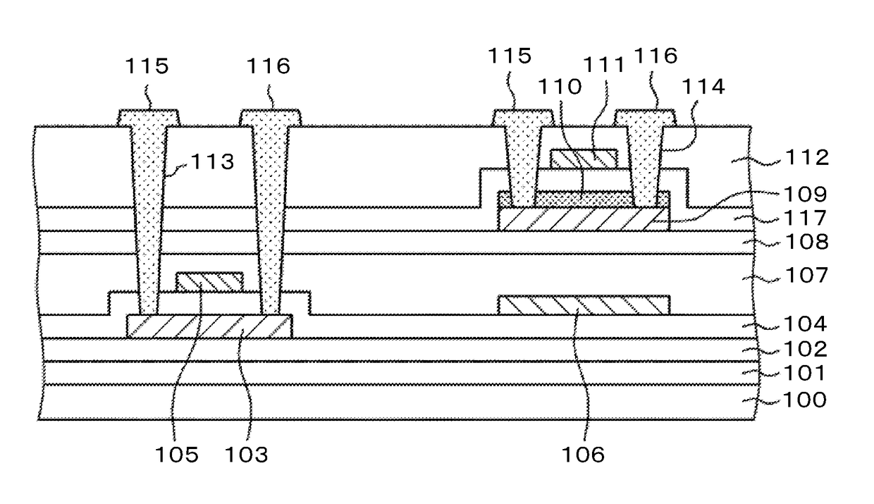
[0072]FIG. 17 is a cross-sectional view showing a second embodiment of the present invention. FIG. 17 differs from FIG. 8 of the first embodiment in that the sacrificial layer 110 covers also the side faces of the TAOS 109. With this configuration, even when hydrofluoric acid permeates toward a side face of the TAOS 109, the side face of the TAOS 109 is protected by the sacrificial layer 110 and the influence on the TAOS 109 can be avoided.

[0073]Consequently, as shown in FIG. 18, the width of the through holes 114 in which the drain electrode 115 and the source electrode 116 are formed can be made larger than the width yy of the sacrificial layer 110. Namely, the channel width of the TFT can be increased and the ON current can be increased.

[0074]Incidentally, while employing a configuration like FIG. 17 for the TAOS 109 and the sacrificial layer 110 leads to an increase in the number of steps, the degree of freedom of the process can be increased. Put another way, the tolerance of t...

third embodiment

[0075]FIG. 19 is a cross-sectional view showing a third embodiment of the present invention. FIG. 19 differs from FIG. 8 of the first embodiment in that the gate insulation film of the TFT made with TAOS 109 is constituted of not only the sacrificial layer 110 but also a gate insulation film 117 made with SiOx. By the addition of the gate insulation film 117 made with SiOx, the degree of freedom of the film thickness of the sacrificial layer 110 made with AlOx can be increased. Put another way, it becomes possible to determine the film thickness and the film quality of the sacrificial layer 110 in consideration not of the insulation characteristic but exclusively of the threshold of the TAOS TFT and the etching characteristic of the sacrificial layer.


PUM

PropertyMeasurementUnit
refractive indexaaaaaaaaaa
thicknessaaaaaaaaaa
thicknessaaaaaaaaaa

Abstract

The object of the present invention is to make it possible to form an LIPS TFT and an oxide semiconductor TFT on the same substrate. A display device includes a substrate having a display region in which pixels are formed. The pixel includes a first TFT using an oxide semiconductor 109. An oxide film 110 as an insulating material is formed on the oxide semiconductor 109. A gate electrode 111 is formed on the oxide film 110. A first electrode 115 is connected to a drain of the first TFT via a first through hole formed in the oxide film 110. A second electrode 116 is connected to a source of the first TFT via a second through hole formed in the oxide film 110.

Description

CLAIM OF PRIORITY[0001]The present application claims priority from Japanese Patent Application JP 2016-100493 filed on May 19, 2016, the content of which is hereby incorporated by reference into this application.BACKGROUND OF THE INVENTION1. Field of the Invention[0002]The present invention relates to a display device, and in particular, to a display device employing hybrid structure formed of both a TFT using poly-Si and a TFT using an oxide semiconductor.2. Description of the Related Art[0003]In a liquid crystal display device, a TFT substrate on which pixels each having pixel electrodes, a thin-film transistor (TFT), etc. are formed like a matrix and a counter substrate are arranged to face each other and a liquid crystal is sandwiched between the TFT substrate and the counter substrate. The liquid crystal display device forms an image by controlling the light transmittance of liquid crystal molecules in regard to each pixel. On the other hand, an organic electroluminescence (EL...

Claims


Application Information

Patent Timeline
Patent Type & Authority Applications(United States)
IPC IPC(8): H01L27/12H01L29/51G02F1/1362G02F1/1368G02F1/133H01L29/786H01L29/24H01L27/32
CPCH01L27/1225G02F2202/104H01L27/1251H01L29/78633H01L29/517H01L29/24H01L29/7869H01L29/78675G02F1/1368G02F1/13306G02F1/136209H01L27/3262G02F2202/10G02F2001/13685H01L27/1222H01L27/1259H01L29/78693H01L29/41733H01L29/42384H01L29/4908G02F1/13685H10K59/1213
Inventor SUZUMURA, ISAOWATABE, KAZUFUMIISHII, YOSHINORIMIYAKE, HIDEKAZUYAMAGUCHI, YOHEI
Owner JAPAN DISPLAY INC
Why Eureka
Try Eureka