

Method for manufacturing a bonded soi wafer
a technology of bonded soi and bonded film, which is applied in the direction of basic electric elements, electrical apparatus, and semiconductor devices, can solve the problems of reducing the thermal conductivity of the operating radio-frequency device, unable to remove the generated heat, and oxide films, etc., and achieves the effects of reducing the generation of voids, high quality, and high productivity
Active Publication Date: 2017-11-30
SHIN-ETSU HANDOTAI CO LTD
View PDF4 Cites 27 Cited by
- Summary
- Abstract
- Description
- Claims
- Application Information
AI Technical Summary
Benefits of technology
The patent describes a method for making a bonded SOI wafer which has a flat surface and minimal voids after polishing. This method reduces the number of polishing steps required, resulting in a high quality bonded SOI wafer at a low cost.
Problems solved by technology
Oxide films, however, has lower thermal conductivity, and cannot remove the generated heat in operating radio-frequency devices.
At this portion, electric conduction is generated to make it impossible to control harmonics.
Method used
View moreImage
Smart ImageViewing Examples

Examples
examples
[0068]Hereinafter, the present invention will be more specifically described by showing Example and Comparative Examples, but the present invention is not limited thereto.
Login to View More PUM
| Property | Measurement | Unit |
|---|---|---|
| resistivity | aaaaa | aaaaa |
| surface roughness | aaaaa | aaaaa |
| diameter | aaaaa | aaaaa |
Abstract
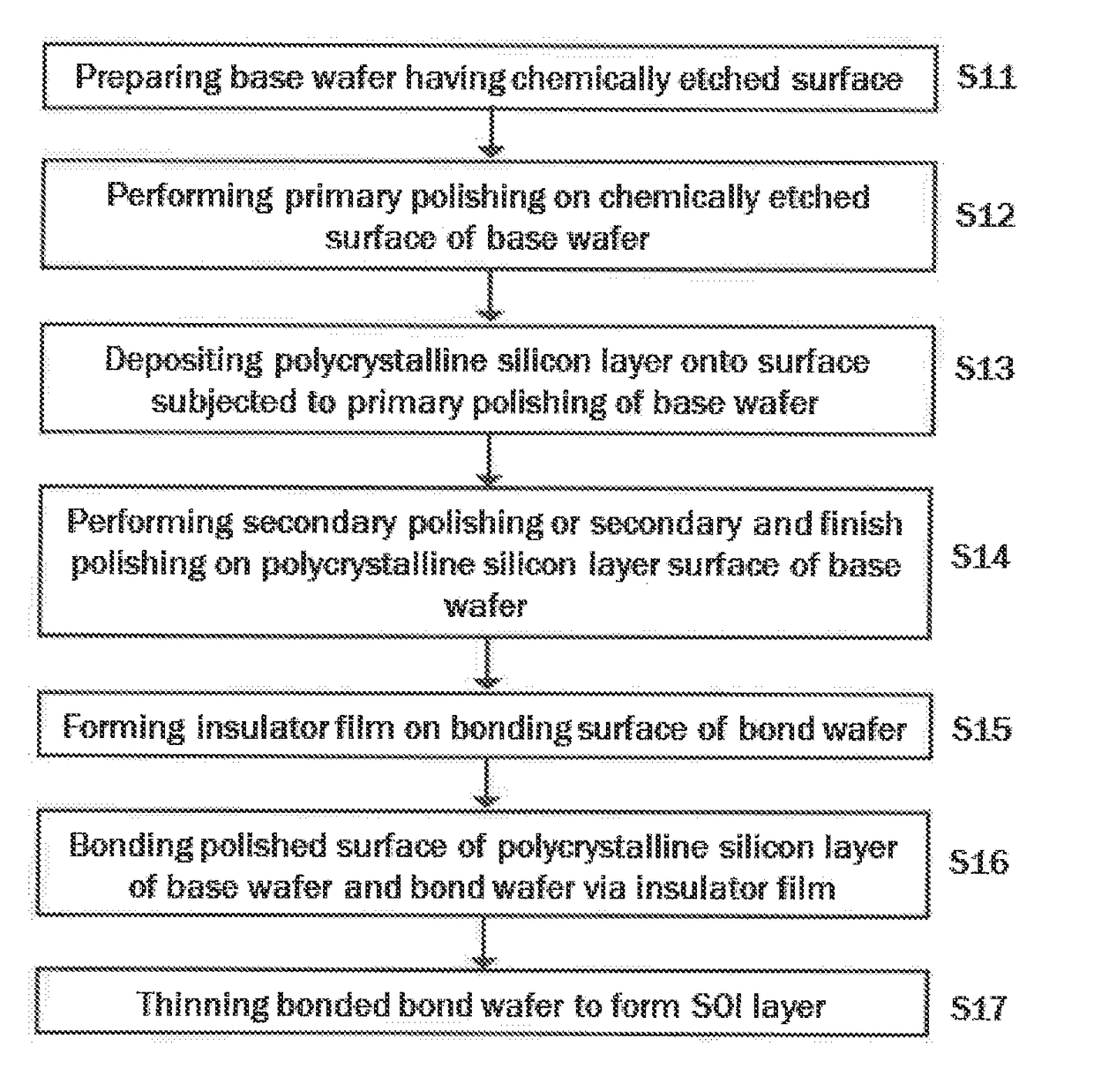
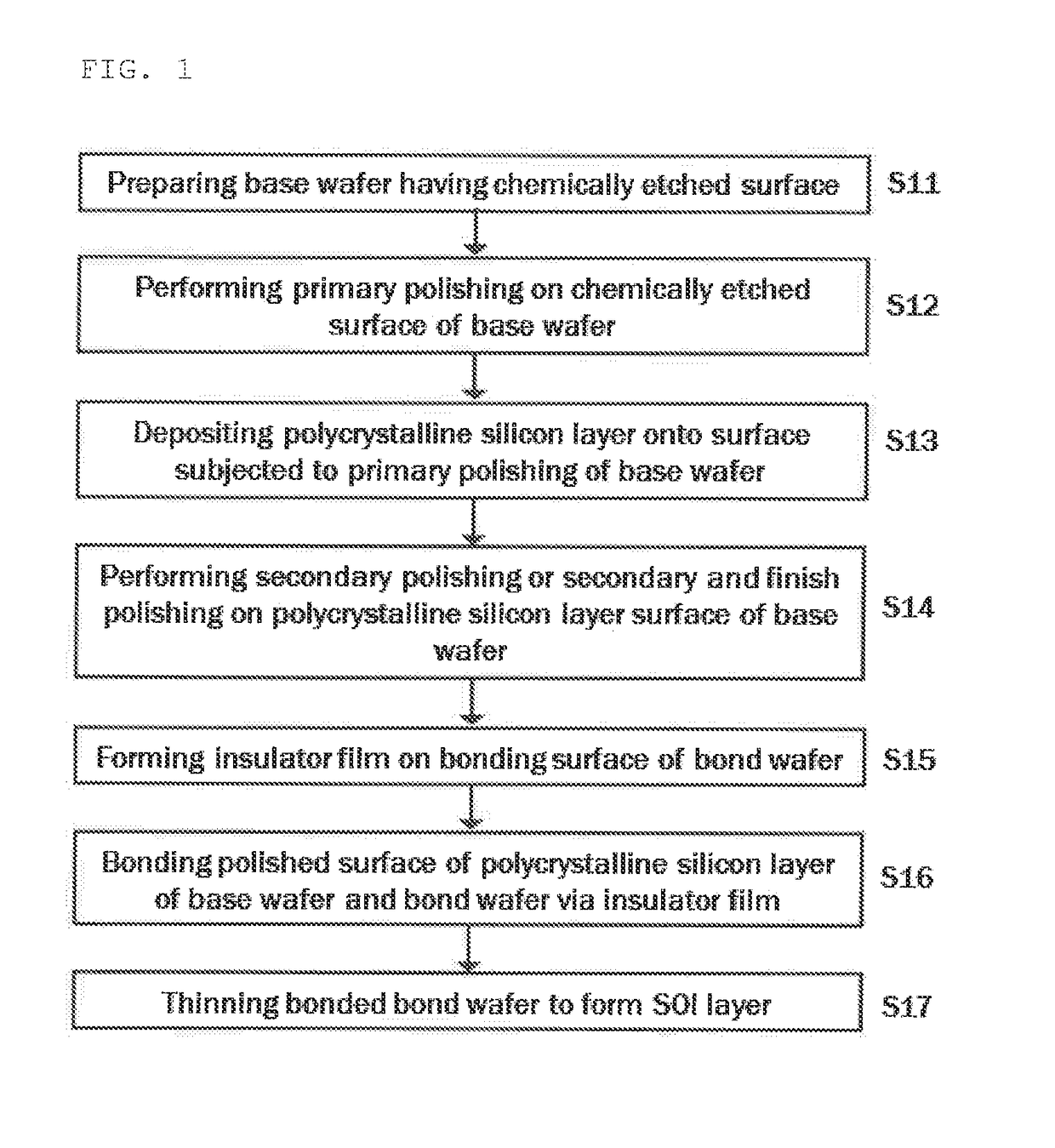
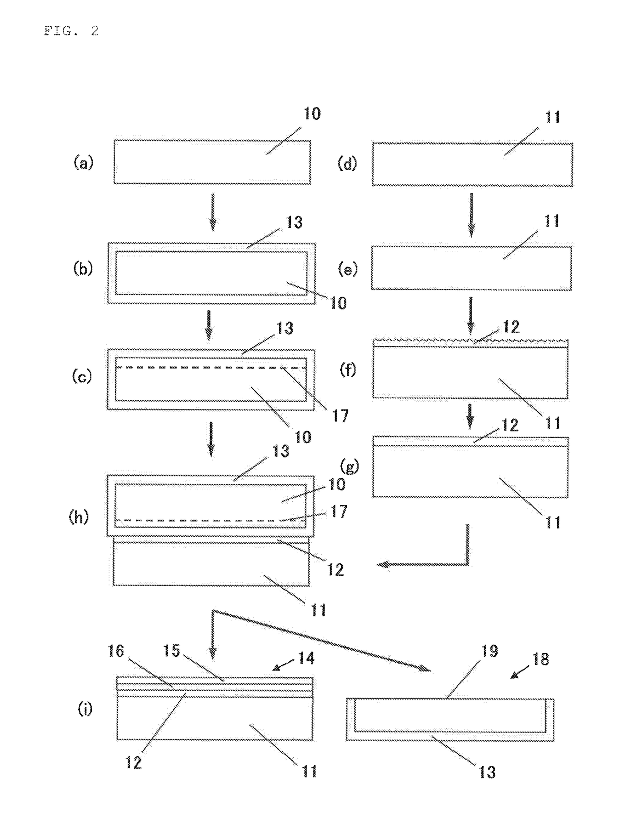
Method for manufacturing a bonded SOI wafer by bonding a bond wafer and base wafer, each composed of a silicon single crystal, via an insulator film, including the steps: depositing a polycrystalline silicon layer on the base wafer bonding surface side, polishing the polycrystalline silicon layer surface, forming the insulator film on the bonding surface of the bond wafer, bonding the polished surface of the base wafer polycrystalline silicon layer and bond wafer via the insulator film; thinning the bonded bond wafer to form an SOI layer; wherein, in the step of depositing the polycrystalline silicon layer, a wafer having a chemically etched surface as base wafer; chemically etched surface is subjected to primary polishing followed by depositing the polycrystalline silicon layer on surface subjected to the primary polishing, and in the step polishing the polycrystalline silicon layer surface, which is subjected to secondary polishing or secondary and finish polishing.
Description
TECHNICAL FIELD[0001]The present invention relates to a method for manufacturing a bonded SOI wafer.BACKGROUND ART[0002]With developments of portable terminals, internet communication, etc., wireless communication has been receiving more and more increasing demands for the amounts of information and the communication speeds. As radio-frequency devices such as RF switches, miniaturization and integration technology has been increasingly adopted recently to substitute single devices, each of which have been made of a substrate such as an SOS (Silicon On Sapphire) substrate and a GaAs substrate, to a device that integrate these single devices onto an Si substrate. Particularly, methods for manufacturing radio-frequency devices by using SOI wafers have been largely extending a market.[0003]As properties of radio-frequency devices, suppression of second harmonic and third harmonic have been a main requirement to prevent a crossed line of communication. To fulfil this requirement, the sub...
Claims
Login to View More Application Information
Patent Timeline
 Patent Type & AuthorityApplications(United States)
IPC IPC(8): H01L21/304H01L27/12H01L21/04
CPCH01L21/304H01L27/1203H01L21/0445H01L21/02H01L27/12H01L21/3212H01L21/02024H01L21/76254H01L21/02008H01L21/02107H01L21/02013H01L21/02104H01L21/02019H01L21/02595H01L21/02499
InventorISHIZUKA, TORUKOBAYASHI, NORIHIRONAKANO, MASATAKE
OwnerSHIN-ETSU HANDOTAI CO LTD