Semiconductor-encapsulating adhesive, semiconductor-encapsulating film-form adhesive, method for producing semiconductor device, and semiconductor device

a technology of semiconductor encapsulation and adhesive, which is applied in the direction of adhesive types, adhesive types, and basic electric elements, can solve the problems of air bubbles called voids, and achieve the effects of reducing the generation of voids, excellent connection reliability, and excellent connection reliability

Active Publication Date: 2012-01-19
RESONAC CORP
View PDF3 Cites 7 Cited by
  • Summary
  • Abstract
  • Description
  • Claims
  • Application Information

AI Technical Summary

Benefits of technology

[0025]Another embodiment of the present invention is a semiconductor-encapsulating film-form adhesive obtained by forming the semiconductor-encapsulating adhesive of the above-mentioned embodiment into a film-form shape. Use of such a semiconductor-encapsulating film-form adhesive, since the semiconductor-encapsulating adhesive of the above-mentioned embodiment is used, can suppress the generation of voids even in connection at a high temperature of 300° C. or higher, and can produce a semiconductor exhibiting an excellent connection reliability.
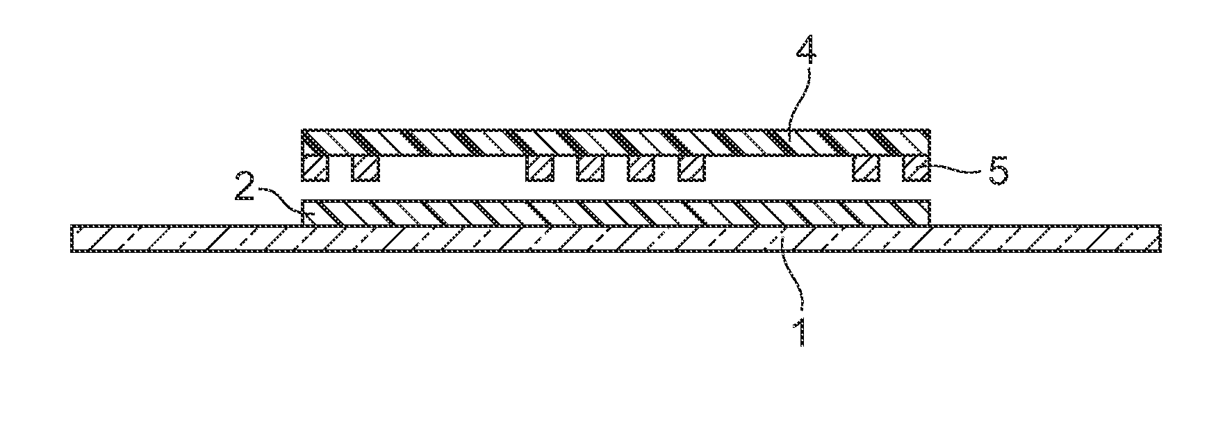
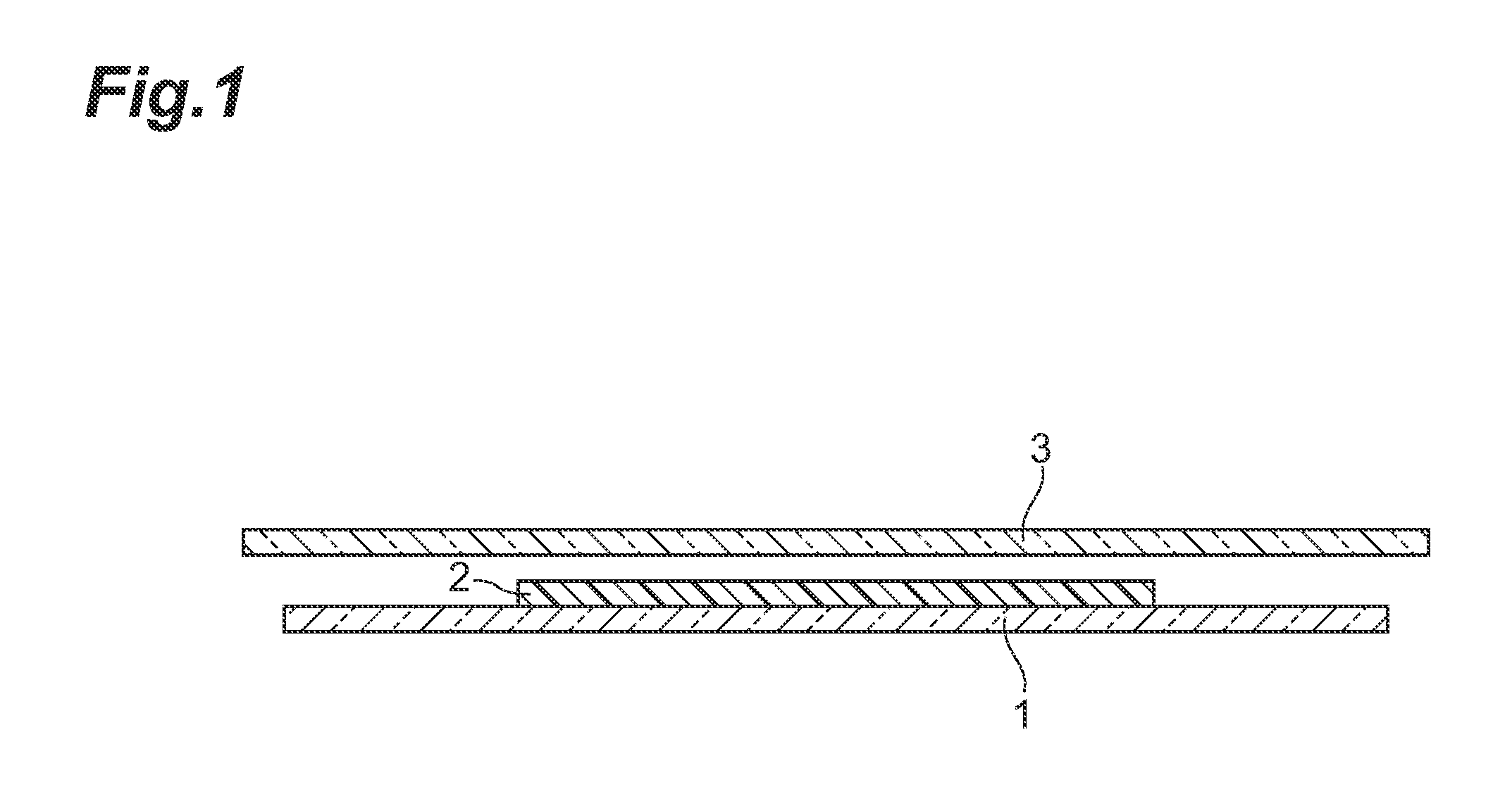
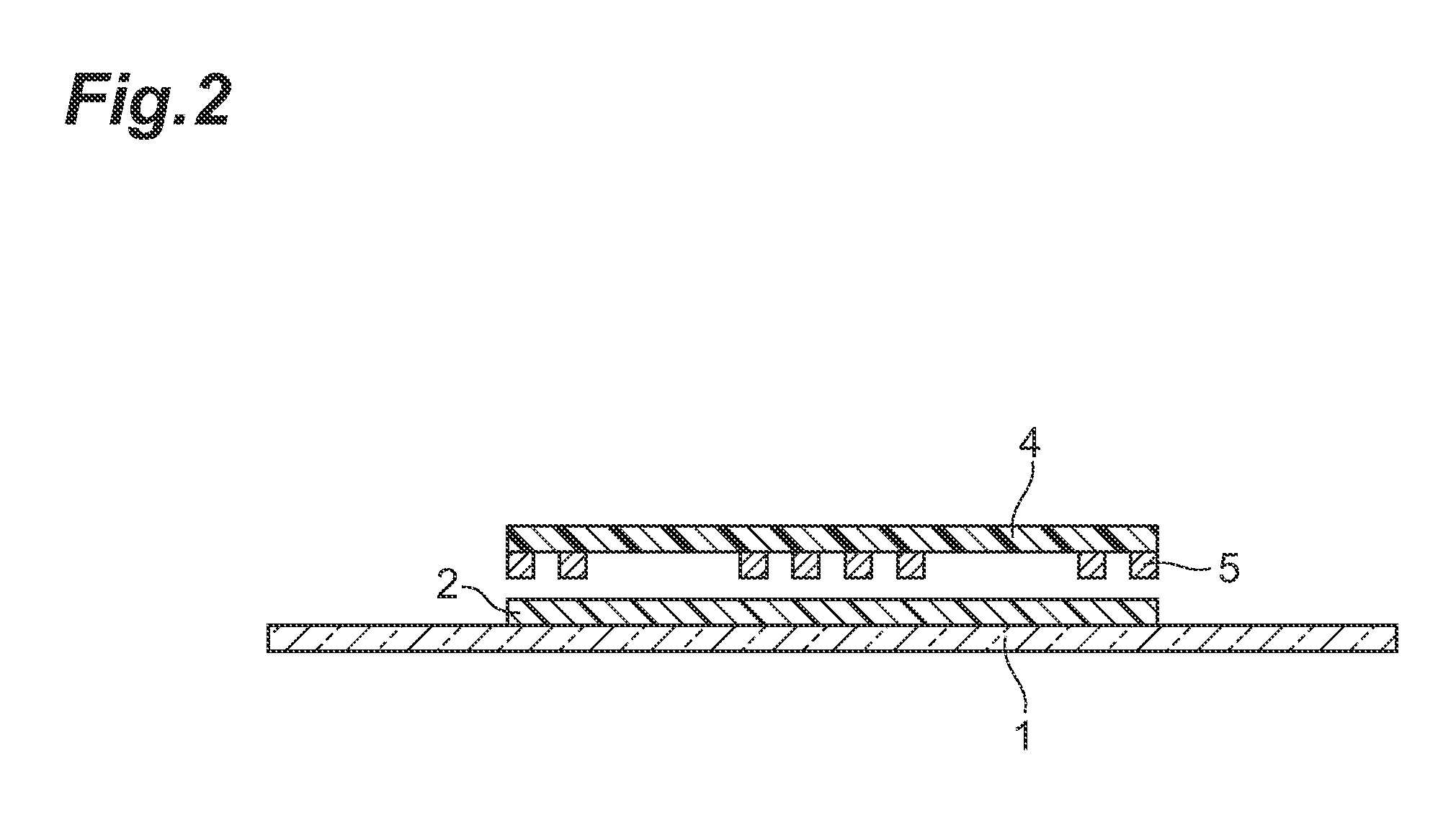
[0026]A method for producing a semiconductor device as further another embodiment of the present invention is a producing method of a semiconductor device equipped with a semiconductor chip having bumps and a substrate having metal interconnects, and comprises a connection step of arranging the semiconductor chip and the substrate such that the bumps and the metal interconnects face each other with the semiconductor-encapsulating adhesive or the semiconductor-encapsulating film-form adhesive of the embodiment interposed, and heating the semiconductor chip and the substrate while pressing them in the facing direction thereof, to cure the semiconductor-encapsulating adhesive or the semiconductor-encapsulating film-form adhesive and to electrically connect the bumps and the metal interconnects. In the connection step, the bumps and the interconnects may be electrically connected by heating the semiconductor chip and the substrate to 300° C. or higher while pressing them in the facing direction thereof to form a gold-tin eutectic between the bumps containing gold and the metal interconnects having a tin-coated layer. Such a method for producing a semiconductor device, since using the semiconductor-encapsulating adhesive or the semiconductor-encapsulating film-form adhesive, can produce a semiconductor device having excellent connection reliability.
[0027]A semiconductor device as another embodiment of the present invention can be produced by the producing method of the above-mentioned embodiment. Such a semiconductor device, since produced by the producing method of the embodiment, has excellent connection reliability.

Problems solved by technology

However, in the case where the connection of COF is carried out by this method, volatile components in an adhesive foam due to a high temperature of 300° C. or higher in connection and are likely to generate air bubbles called voids.

Method used


Image

  • Semiconductor-encapsulating adhesive, semiconductor-encapsulating film-form adhesive, method for producing semiconductor device, and semiconductor device
  • Semiconductor-encapsulating adhesive, semiconductor-encapsulating film-form adhesive, method for producing semiconductor device, and semiconductor device
  • Semiconductor-encapsulating adhesive, semiconductor-encapsulating film-form adhesive, method for producing semiconductor device, and semiconductor device

Examples


examples

[0091]Hereinafter, one embodiment of the present invention will be described specifically by way of Examples, but the scope of the present invention is not limited to Examples.

[0092](Synthesis of a Polyimide Resin)

[0093]In a 300-ml flask equipped with a thermometer, a stirrer, and a calcium chloride tube, 2.10 g (0.035 mol) of 1,12-diaminododecane, 17.31 g (0.03 mol) of a polyether diamine (ED2000, made by BASF AG, ), 2.61 g (0.035 mol) of 1,3-bis(3-aminopropyl)tetramethyldisiloxane (LP-7100, made by Shin-Etsu Chemical Co., Ltd.) and 150 g of N-methyl-2-pyrrolidone (made by Kanto Chemical Co., Inc.) were charged and stirred. After the diamine was dissolved, 15.62 g (0.10 mol) of 4,4′-(4,4′-isopropylidenediphenoxy)bis(phthalic dianhydride) (BPADA, made by Sigma-Aldrich Corp.) having been recrystallization refined with acetic anhydride was added little by little while the flask was being cooled in an ice bath. After the solution was allowed to react at room temperature (25° C.) for 8 ...

examples 1 and 2

, Comparative Examples 1 to 4, and Experimental Examples 1 to 3

[0098]Film-form adhesives were fabricated by the same method as that for the above-mentioned film-form adhesive, except for altering to compositions of materials used shown in Table 1.

[0099]Compounds used in Examples, Comparative Examples and

[0100]Experimental Examples are as follows.

(a) Epoxy Resins

[0101]A cresol novolac epoxy resin (YDCN-702, made by Tohto Kasei Co., Ltd.)

[0102]A polyfunctional special epoxy resin (VG3101L, made by Printec Corporation)

[0103]Triphenolmethane polyfunctional solid epoxy resin (Japan Epoxy Resins Co., Ltd., EP1032H60)

(b) Compounds Formed of an Organic Acid Reactive with an Epoxy Resin and a Curing Accelerator

[0104]1-cyanoethyl-2-phenylimidazolium trimellitate (2PZ-CNS, made by Shikoku Chemicals Corp.)

[0105]1-cyanoethyl-2-undecylimidazolium trimellitate (C11Z-CNS, made by Shikoku Chemicals Corp.)

[0106]Synthesized curing accelerator 1

[0107]Synthesized curing accelerator 2

(b′) Curing Accelera...


PUM

PropertyMeasurementUnit
melting pointaaaaaaaaaa
melt viscosityaaaaaaaaaa
eutectic temperatureaaaaaaaaaa

Abstract

The present invention relates to a semiconductor-encapsulating adhesive, a semiconductor-encapsulating film-form adhesive, a method for producing a semiconductor device, and a semiconductor device. The present invention provides a semiconductor-encapsulating adhesive comprising (a) an epoxy resin, and (b) a compound formed of an organic acid reactive with an epoxy resin and a curing accelerator.

Description

[0001]The present application corresponds to Japanese Application No. 2008-262100, filed Oct. 8, 2008, which was published as Japanese Application No. 2009-256587, on Nov. 5, 2009, the entire disclosures of the above applications are hereby, incorporated by reference.BACKGROUND OF THE INVENTION[0002]1. Field of the Invention[0003]The present invention relates to a semiconductor-encapsulating adhesive, a semiconductor-encapsulating film-form adhesive, a method for producing a semiconductor device, and a semiconductor device.[0004]2. Related Background Art[0005]Heretofore, as a method for producing a semiconductor device, the wire bonding system, which uses metal fine wire such as gold wire, has been broadly applied in order to connect semiconductor chips and substrates. On the other hand, in order to meet requirements of miniaturization, thickness reduction and high functionality for semiconductor devices, the flip chip connection systems have recently been spreading in which conduct...

Claims


Application Information

Patent Timeline
Patent Type & Authority Applications(United States)
IPC IPC(8): H01L23/28C09J163/04C09J179/08H01L21/56
CPCH01L2924/01029H01L2924/0103H01L2924/01047H01L2924/0105H01L2924/01079C09J163/04C09J179/08H01L21/563H01L23/293H01L24/29H01L2224/2919H01L2224/73204H01L2924/01012H01L2924/01013H01L2924/01005H01L2924/01006H01L2924/0102H01L2924/01023H01L2924/01033H01L2924/01322H01L2924/014H01L2924/0665H01L2224/29101C08G59/42C09J163/00H01L24/73H01L24/81H01L24/83H01L2224/13144H01L2224/13155H01L2224/16225H01L2224/2929H01L2224/29386H01L2224/29388H01L2224/29393H01L2224/73104H01L2224/81191H01L2224/81201H01L2224/81411H01L2224/81444H01L2224/81455H01L2224/81805H01L2224/83191H01L2224/83192H01L2224/94H01L2224/81903H01L2924/00013C08L63/00H01L2924/00H01L2224/11H01L2224/27H01L2924/00014H01L2924/05442H01L2924/05432H01L2924/05341H01L2924/0503H01L2224/29099H01L2224/29199H01L2224/29299
Inventor HONDA, KAZUTAKAENOMOTO, TETSUYANAKAMURA, YUUKI
Owner RESONAC CORP
Why Eureka
Try Eureka