Soldering alloy and solder joint

a solder alloy and solder joint technology, applied in the direction of soldering apparatus, manufacturing tools, welding/cutting media/materials, etc., can solve the problems of poor wettability of the solder alloy to ti, poor impact resistance and heat cycle resistance of the bonded portion after die bonding, and reduce the generation of voids , the effect of suppressing the generation of ni and generation

Inactive Publication Date: 2020-12-10
SENJU METAL IND CO LTD
View PDF0 Cites 0 Cited by
  • Summary
  • Abstract
  • Description
  • Claims
  • Application Information

AI Technical Summary

Benefits of technology

[0016]Next, in order to suppress the generation of voids at a bonded interface, the present inventors focused on the P content. P is known to take in oxygen in the atmosphere when coexisting with Sn to form tin phosphate. Tin phosphate is formed as a brittle and thin oxide film on a surface of the molten solder. This oxide film can be easily broken by convection of the molten solder itself and / or an external pressure applied to the molten solder when placing the chip on the molten solder, so that the oxide film may not block convection of the molten solder. For this reason, it is possible in the solder alloy containing P to discharge voids generated at a bonded interface to the outside. In order to suppress elution of Ni and generation of voids, Co, Ni, and P should be blended in a well-balanced manner.
[0017]Furthermore, since the addition of Ag precipitates Ag3Sn at a crystal grain boundary and improves the strength of the solder alloy, it is necessary to further consider the balance of the Ag content.
[0018]Therefore, the present inventors have studied Sn—Ag—Cu—Ni—Co—P solder alloy in detail under consideration of a total balance of a content ratio of Co and Ni, the P content and the Ag content. As a result, the present inventors have found that they show high tensile strength and suppress the generation of elution of Ni and voids, thereby completing the present invention.

Problems solved by technology

When the Ti layer is exposed due to progress of elution of Ni, the wettability of the molten solder is repelled by the back metal because the wettability of the solder alloy to Ti is very poor.
As a result, the bonded portion after die bonding may be inferior in impact resistance and heat cycle resistance.

Method used


Image

  • Soldering alloy and solder joint

Examples


Embodiment Construction

"d_n">[0026]The present invention is described in more detail below. In the present specification, the unit “%” for the solder alloy composition refers to “mass %” unless otherwise specified.

[0027]1. Alloy Composition

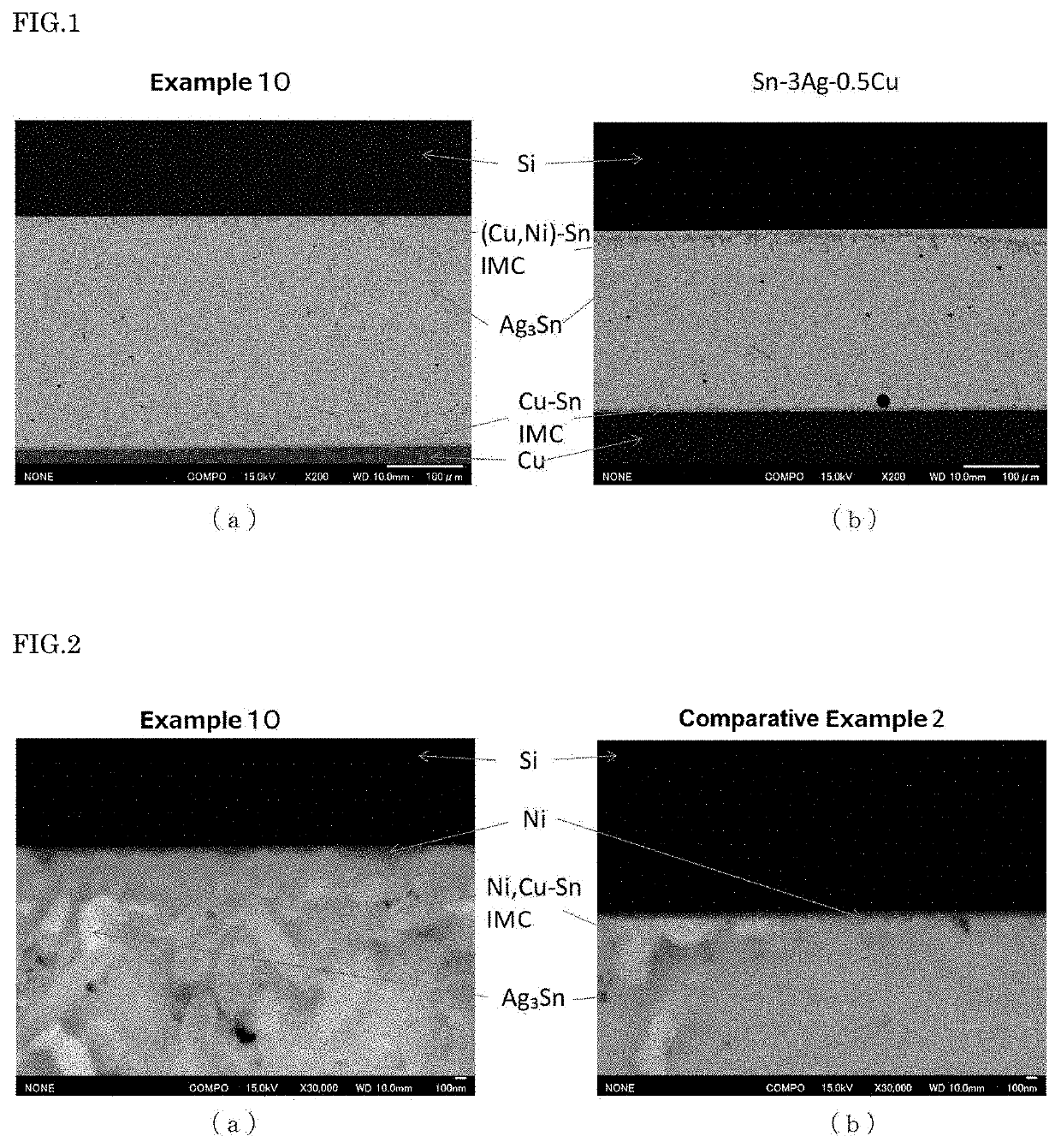
[0028](1) Ag: 1 to 4%

[0029]Ag is an element that improves the strength of the solder alloy by precipitating fine Ag3Sn at crystal grain boundaries. If the Ag content is less than 1%, an effect of adding Ag is not sufficiently exhibited. The lower limit of the Ag content is 1% or more, preferably 1.5% or more, and more preferably 2% or more. On the other hand, when the Ag content is too large, coarse Ag3Sn is precipitated, as a result, the strength is reduced. The upper limit of the Ag content is 4% or less, preferably 3.5% or less, and more preferably 3% or less.

[0030](2) Cu: 0.1 to 1.0%

[0031]Cu is an element that can suppress elution of Cu and enable precipitation strengthening by Cu6Sn5. If the Cu content is less than 0.1%, a small amount of Cu6Sn5 and a brittle SnNi ...


PUM

PropertyMeasurementUnit
liquidus temperatureaaaaaaaaaa
solidus temperatureaaaaaaaaaa
liquidus temperatureaaaaaaaaaa

Abstract

The present invention provides a solder alloy and a solder joint which have high tensile strength, can suppress elution of Ni, and can suppress generation of voids at a bonded interface. A solder alloy includes an alloy composition constituted from Ag: 1 to 4%, Cu: 0.1 to 1.0%, 0.005 to 0.09%, Co: 0.0025 to 0.1%, P: 0.001 to 0.015% by mass % and a balance Sn, wherein the alloy composition fulfills the following formula (1): 0.00020<(Ni/Co)·(1/Ag)·P<0.025 (1), wherein Ni, P, Ag and Co represent contents (mass %) of the alloy composition respectively.

Description

BACKGROUND OF THE INVENTIONTechnical Field[0001]The present invention relates to a solder alloy and a solder joint having high tensile strength and suppressing generation of elution of Ni and voids at a bonded interface.Background Art[0002]In recent years, electronic devices have been required to have higher integration, larger capacity and higher speed. For example, a semiconductor package such as a QFP (Quad Flat Package) is used, and it has been attempted to achieve higher integration and higher functionality at a semiconductor chip level. In manufacture of QFP, a packaging process of die bonding a silicon chip cut from a silicon wafer to a lead frame is employed.[0003]For a QFP in which microelectrodes such as BGA (Ball Grid Array) are bonded, a silicon chip and a lead frame are die-bonded with a solder alloy to form a solder joint. For example, a back metal having a Ni layer as an outermost layer is formed on the silicon chip in order to improve wettability with solder and impr...

Claims


Application Information

Patent Timeline
Patent Type & Authority Applications(United States)
IPC IPC(8): B23K35/26
CPCB23K35/262B23K2103/08C22C13/00
Inventor SAKAMOTO, TAKESHIKOGA, SHUNSUKETAGUCHI, TOSHIHIKO
Owner SENJU METAL IND CO LTD
Why Eureka
Try Eureka