Power device and method for fabricating thereof

a power device and transistor technology, applied in the field of gall, can solve problems such as foreseeable optimization limitations, and achieve the effect of increasing the effective gate width and increasing the channel conductivity per unit length

Inactive Publication Date: 2017-11-30
EPISTAR CORP
View PDF7 Cites 15 Cited by
  • Summary
  • Abstract
  • Description
  • Claims
  • Application Information

AI Technical Summary

Benefits of technology

[0006]Another object of the present application is to provide a HEMT that is a AlGaN / GaN HEMT having a patterned three-dimensional gate geometry for achieving increased effective gate width so as to obtain increased channel conductivity per unit length.

Problems solved by technology

Based on existing techniques for increasing the effective width of the gate for achieving increased channel conductivity per unit length, a foreseeable optimization limitation can be reached.

Method used


Image

  • Power device and method for fabricating thereof
  • Power device and method for fabricating thereof
  • Power device and method for fabricating thereof

Examples


Embodiment Construction

[0037]The present application will now be described more specifically with reference to the following embodiments. It is to be noted that the following descriptions of the embodiments of this invention are presented herein for purpose of illustration and description only. It is not intended to be exhaustive or to be limited to the precise form disclosed.

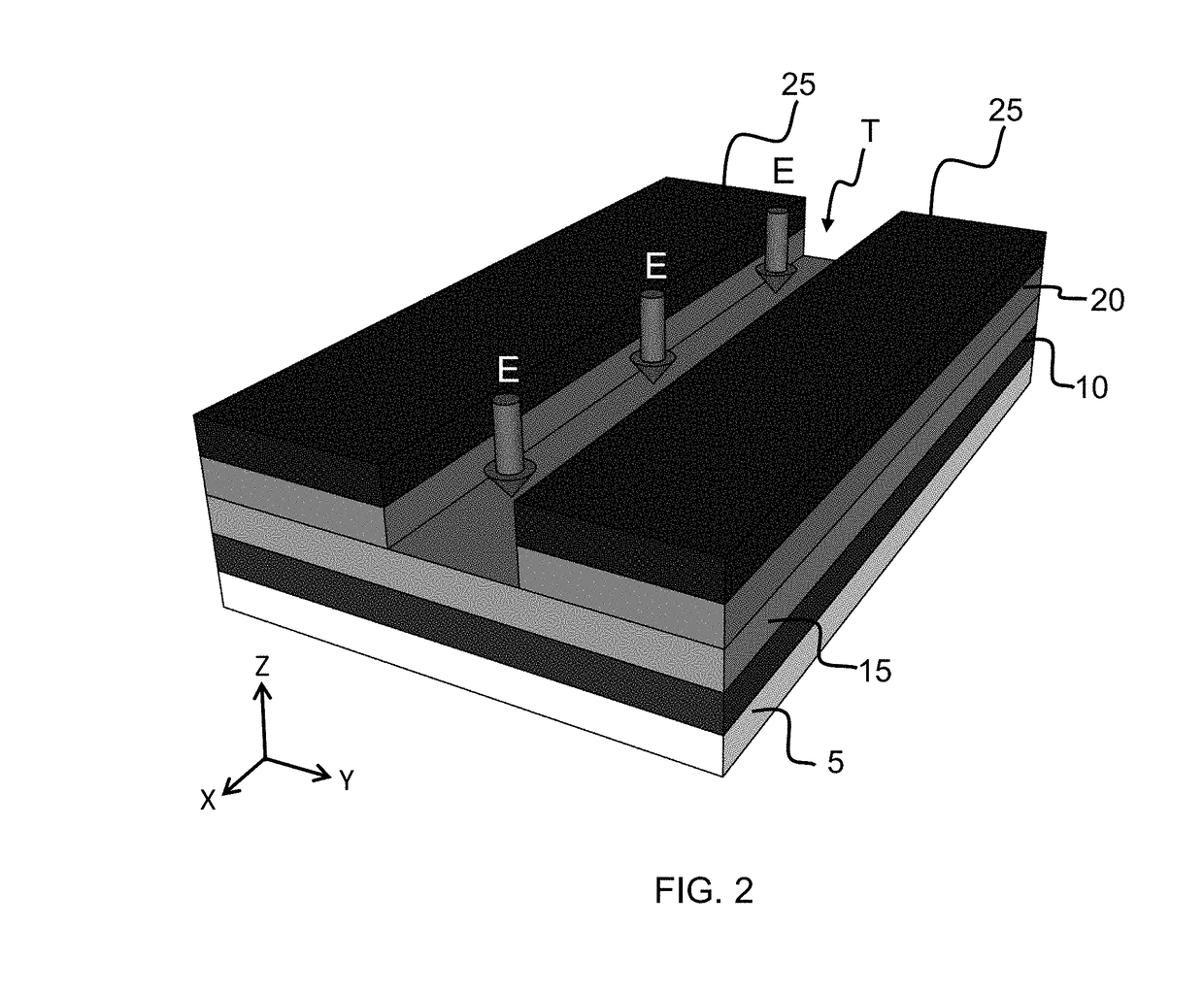
[0038]As shown in FIGS. 2-10, 12-13, 15-22, a three-dimensional Cartesian coordinate system, with axis lines (or axis directions) X, Y and Z, oriented as shown by the arrows are utilized for describing various directions and orientations of elements and device structures to the following embodiments.

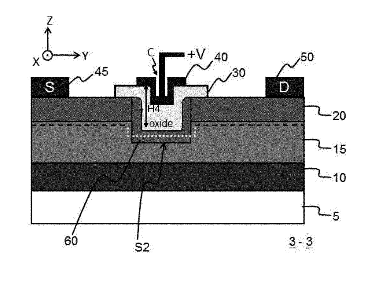
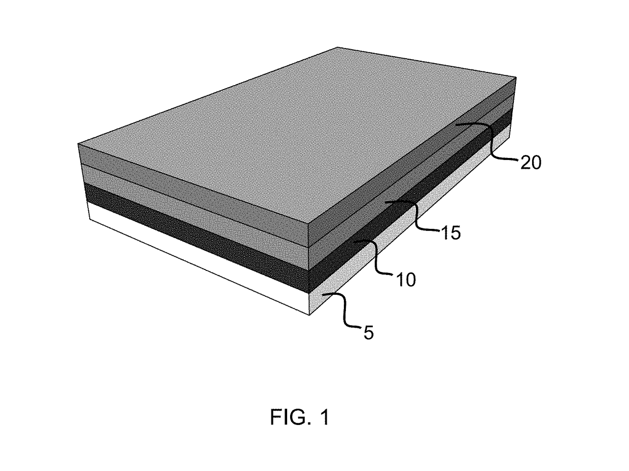
[0039]In accordance with a method for fabricating a power device of an embodiment of present application, referring to FIGS. 1-10 and 22, a power device, which is a HEMT having a patterned three-dimensional gate geometry, is fabricated by means of the following steps. As shown in FIG. 1, in step (a), a buffer layer 10, a channel layer 15,...


PUM


Abstract

A power device having a patterned three-dimensional gate geometry is fabricated and described. The power device achieved increased effective gate width and increased channel conductivity per unit length. It includes at least a channel layer, a barrier layer, a dielectric layer, a gate disposed on the dielectric layer, dielectric layer disposed on the barrier layer and the channel layer, respectively. Gate includes protruding sections and extending sections directly contacting the dielectric layer. Dielectric layer includes a repeating rectangular-wave structure. The dielectric layer forms a gate oxide directly contacting trenches of channel layer. Alternatively, gate oxide can be disposed directly on a p-doped GaN filled region which includes an alternating repeating rectangular-wave structure.

Description

BACKGROUND OF THE INVENTION(a) Field of the Invention[0001]The present application is related to a high-electron-mobility transistor (HEMT) power device, and more particularly, to a gallium nitride (GaN) high-electron-mobility transistor (HEMT) having a patterned three-dimensional gate geometry.(b) Description of the Prior Art[0002]Gallium nitride (GaN) had been used extensively as a light illuminating material, and has been used as a main material for fabricating commercial blue LEDs. Meanwhile, GaN is also known to be a material of wider bandgap to be used for fabricating a high-electron-mobility transistor (HEMT).[0003]The high-electron-mobility transistor (HEMT) is a field-effect transistor (FET) that has superior electron mobility, high breakdown voltage, and used for creating switching power devices for various applications, such as for motor drive and power supply applications. HEMT made from GaN typically are of AlGaN / GaN heterostructure. GaN is a material that produces spon...

Claims


Application Information

Patent Timeline
Patent Type & Authority Applications(United States)
IPC IPC(8): H01L29/778H01L29/06H01L29/20H01L29/66
CPCH01L29/7787H01L29/66462H01L29/0657H01L29/2003H01L29/4236H01L29/7786H01L29/1037H01L29/1066
Inventor FENG, TIAN-JING
Owner EPISTAR CORP
Why Eureka
Try Eureka