Semiconductor device

a technology of semiconductor devices and semiconductors, applied in semiconductor devices, semiconductor/solid-state device details, electrical apparatus, etc., can solve problems such as delamination, reducing reliability, and slipping, and achieve the effect of improving reliability

Active Publication Date: 2017-12-07
CHIPMOS TECH INC
View PDF1 Cites 3 Cited by
  • Summary
  • Abstract
  • Description
  • Claims
  • Application Information

AI Technical Summary

Benefits of technology

[0005]The invention provides a semiconductor device having convex patterns, which can reduce the phenomenon of peeling, de-lamination, or crack between the RDL and the protective layer thereunder, thereby improving the reliability.
[0026]Based on the above, by forming the convex patterns composed of dielectric materials under the bump in the invention, the metal layer (may be the RDL or the under-bump metal layer, for example) between the bump and the convex patterns has the uneven surface. Thus, compared to the conventional flat surface, the embodiment can improve stress release of the metal layer and reduce transverse thermal expansion effects. That is, the embodiment can reduce the phenomenon of peeling, de-lamination, or crack between the metal layer and the protective layer thereunder, thereby improving the reliability.

Problems solved by technology

Particularly, when the metal copper is used in a larger area (e.g., the pad or the RDL), the phenomenon of expansion of the metal copper is more obvious, which may easily cause the phenomenon of peeling, de-lamination, or crack between the RDL and a protective layer thereunder, thereby reducing the reliability.

Method used


Image

  • Semiconductor device
  • Semiconductor device
  • Semiconductor device

Examples


first embodiment

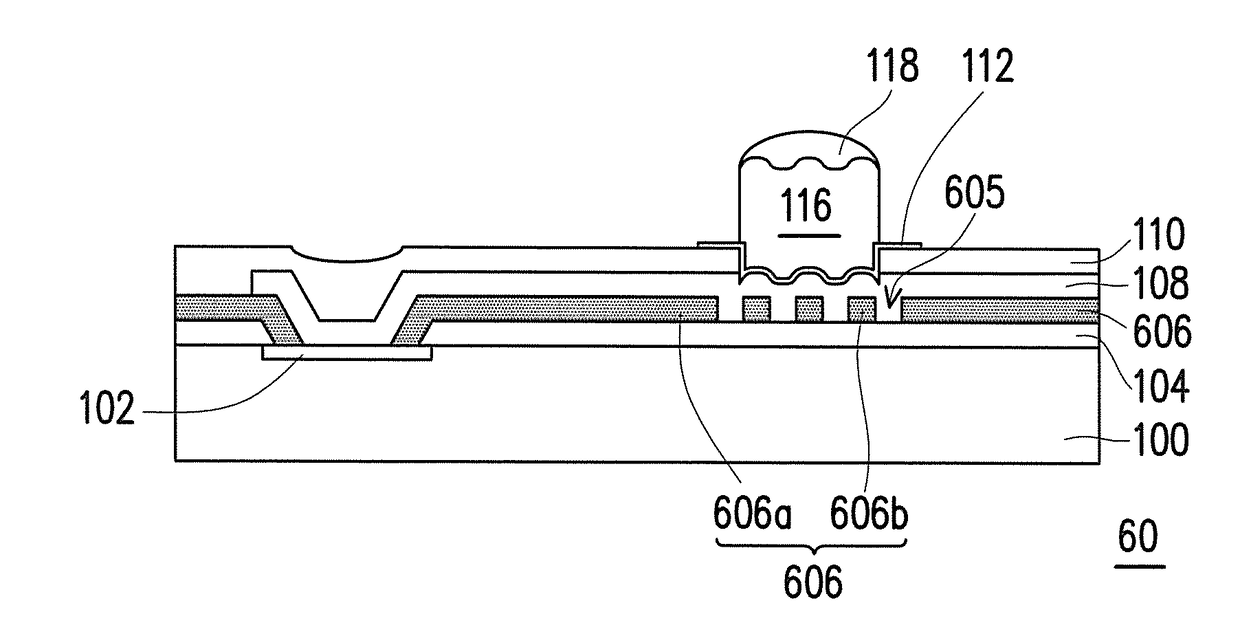
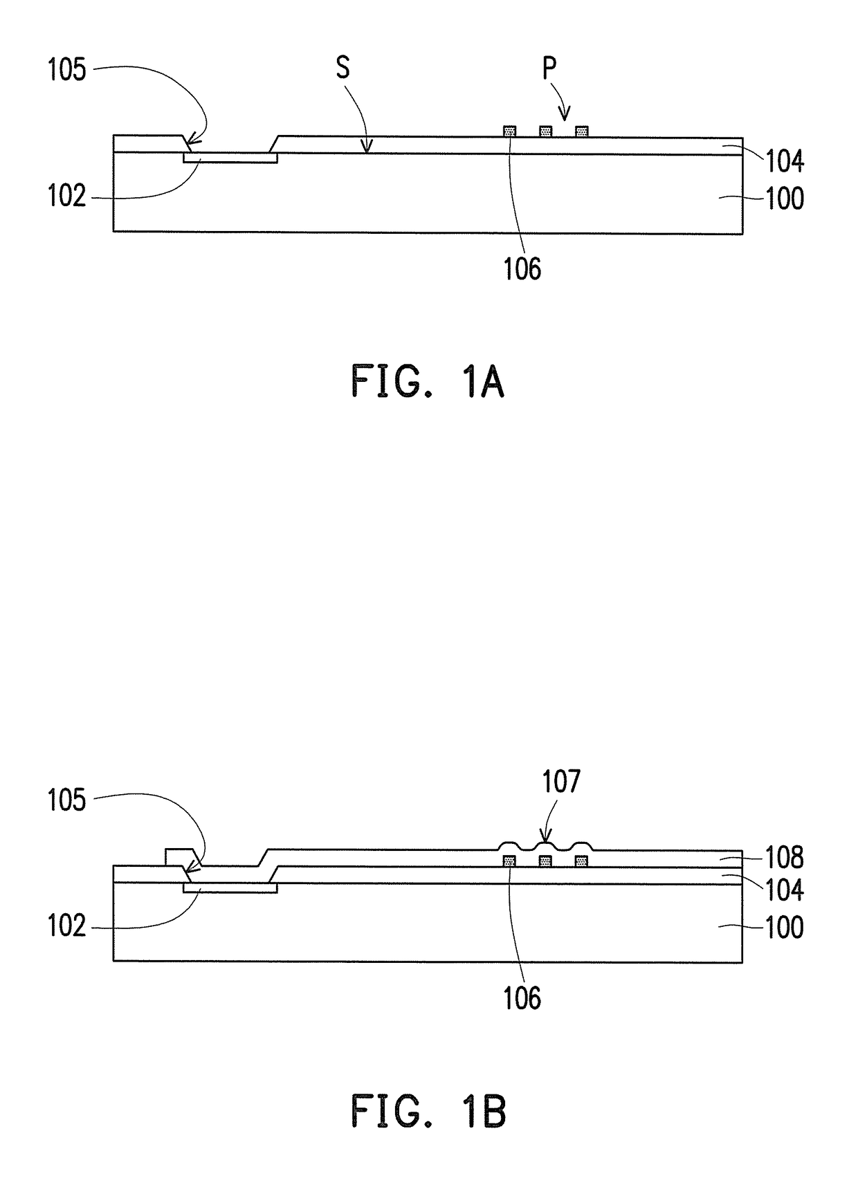
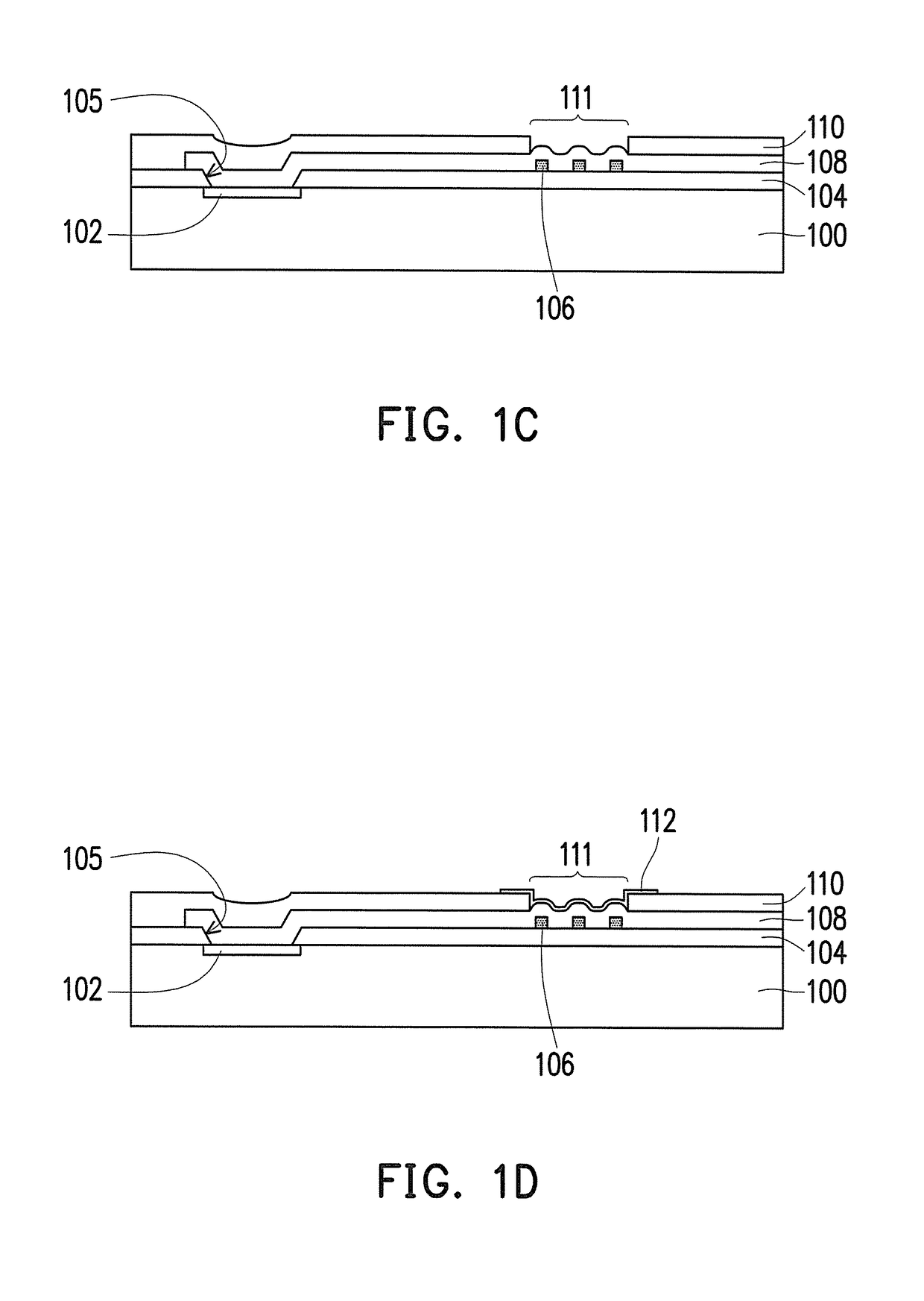
[0037]FIG. 1A to FIG. 1F are schematic cross-sectional diagrams of a manufacturing process of a semiconductor device according to the invention. FIG. 2A to FIG. 2B are schematic top views of a portion of FIG. 1A respectively.

[0038]Referring to FIG. 1A, the invention provides the manufacturing process of a semiconductor device 10 of the first embodiment including the following steps. First, a substrate 100 is provided. A material of the substrate 100 may be at least one material selected from the group consisting of Si, Ge, SiGe, GaP, GaAs, SiC, SiGeC, InAs, and InP, for example. The substrate 100 may also be a silicon-on-insulator (SOI) substrate.

[0039]Then, a pad 102 is formed on an active surface S of the substrate 100. In an embodiment, a material of the pad 102 includes a metal material. The metal material may be copper, aluminum, gold, silver, nickel, palladium, or a combination thereof, for example. A method of forming a pad 102 may be physical vapor deposition, for example.

[0...

second embodiment

[0050]FIG. 3 is schematic cross-sectional diagram of a semiconductor device according to the invention.

[0051]Referring to FIG. 3, basically, a semiconductor device 20 of the second embodiment is similar to the semiconductor device 10 of the first embodiment. The difference between the two is that, a bump 216 of the semiconductor device 20 of the second embodiment has a flat surface 217. A method of forming the flat surface 217 may be that, after forming the bump 216, a grinding method is further used to planarize a surface of the bump 216.

third embodiment

[0052]FIG. 4 is schematic cross-sectional diagram of a semiconductor device according to the invention.

[0053]Referring to FIG. 4, basically, a semiconductor device 30 of the third embodiment is similar to the semiconductor device 10 of the first embodiment. The difference between the two is that, the semiconductor device 30 of the third embodiment further includes a dielectric layer 305 disposed between the convex patterns 106 and the protective layer 104. In an embodiment, a material of the dielectric layer 305 is the same or different from the material of the convex patterns 106. For example, both the convex patterns 106 and the dielectric layer 305 may be PI. On the other hand, the dielectric layer 305 may be silicon oxide, and the convex patterns 106 may be PI.


PUM


Abstract

Provided is a semiconductor device including a substrate, a pad, a protective layer, a plurality of convex patterns, a redistribution layer (RDL), and a bump. The pad is disposed on the substrate. The protective layer is disposed on the substrate. The protective layer has a first opening exposing a portion of a surface of the pad. The convex patterns are disposed on the protective layer. The RDL is disposed on the convex patterns. The RDL extends from the pad to the convex patterns. The bump is disposed on the convex patterns.

Description

CROSS-REFERENCE TO RELATED APPLICATION[0001]This application claims the priority benefit of Taiwan application serial no. 105117997, filed on Jun. 7, 2016. The entirety of the above-mentioned patent application is hereby incorporated by reference herein and made a part of this specification.BACKGROUND OF THE INVENTIONField of the Invention[0002]The invention relates to an integrated circuit, and particularly relates to a semiconductor device.Description of Related Art[0003]With the development of technology, increasing degree of integration of semiconductor devices and reducing critical dimensions have gradually become a trend. In this trend, technique of wafer level package structures which provides a sufficient surface region to bear more input / output (I / O) is generated accordingly. Additionally, a redistribution layer (RDL) can also be formed on a semiconductor chip, so as to redistribute pads on the semiconductor chip to any position.[0004]In general, metal copper is mostly used...

Claims


Application Information

Patent Timeline
Patent Type & Authority Applications(United States)
IPC IPC(8): H01L23/00H01L23/498
CPCH01L24/02H01L23/498H01L23/49811H01L24/17H01L2224/1412H01L23/49894H01L2224/0233H01L2224/0236H01L2224/02373H01L23/49838H01L23/485H01L23/3192H01L24/03H01L24/05H01L24/11H01L24/13H01L2224/02125H01L2224/02145H01L2224/02233H01L2224/02255H01L2224/0235H01L2224/02351H01L2224/0345H01L2224/0401H01L2224/05008H01L2224/05022H01L2224/05147H01L2224/05557H01L2224/05558H01L2224/05569H01L2224/05572H01L2224/05573H01L2224/05639H01L2224/05644H01L2224/05655H01L2224/05664H01L2224/05666H01L2224/11462H01L2224/11464H01L2224/1147H01L2224/1184H01L2224/11849H01L2224/13018H01L2224/13022H01L2224/13082H01L2224/13111H01L2224/13144H01L2224/13147H01L2924/00014H01L2924/01074H01L2924/01047H01L2924/014
Inventor CHUANG, KUN-SHU
Owner CHIPMOS TECH INC
Why Eureka
Try Eureka