Bus bar and power electronic device with current shaping terminal connector and method of making a terminal connector

a technology of current shaping terminal and power electronic device, which is applied in the direction of contact member manufacturing, coupling device connection, laminated bus-bar, etc., can solve the problems of cyclic thermal stress on the side of the switch, debonding of the terminal, fatigue cracking,

Active Publication Date: 2017-12-14
GE GLOBAL SOURCING LLC
View PDF10 Cites 5 Cited by
  • Summary
  • Abstract
  • Description
  • Claims
  • Application Information

AI Technical Summary

Benefits of technology

[0011]In an embodiment, a power electronic device includes a heat sink that has a coolant inlet and a coolant outlet, and first and second switch packages, each package having supply terminals and load terminals. The supply terminals of the first and second switch packages are substantially thermally equidistant from the coolant inlet at a first thermal distance, and the load terminals of the first and second switch packages are substantially thermally equidistant from the coolant inlet at a second thermal distance that is less than the first thermal distance. The power electronic device also includes a

Problems solved by technology

Semiconductor power switches, however, are subject to cyclic thermal stresses.
Although durability is a consideration in semiconductor design, electrical design constraints entail that the various layers of the semiconductor power switches are fabricated from materials having differing thermal properties; in particular, differing coefficients of thermal expansion.
As a result, over time, thermal stress can potentially cause delamination, debonding of terminals, or fatigue cracking.
Thermal stress can also cause electrochemical failures such as current filamenting and Kirkendall void formation.
Structural configurations of isothermal switches, however, may present ch

Method used


Image

  • Bus bar and power electronic device with current shaping terminal connector and method of making a terminal connector
  • Bus bar and power electronic device with current shaping terminal connector and method of making a terminal connector
  • Bus bar and power electronic device with current shaping terminal connector and method of making a terminal connector

Examples


second embodiment

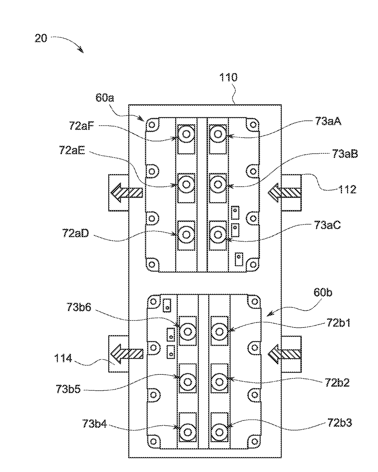
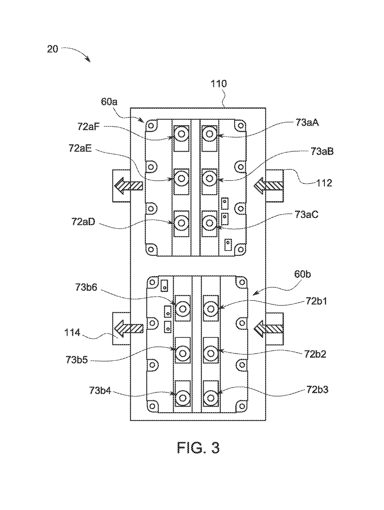
[0052]FIG. 8 illustrates a bus bar, which includes a load terminal connector 800 in combination with supply terminal connectors 810a, 810b. The load terminal connector 800 does not overlap the supply terminal connectors 810a, 810b. The load terminal connector 800 includes a central opening or window 802 from which a slot 804 extends to the edge of the phase plate. The window 802 and the slot 804 divide one or more pre-defined first locations (holes) A, B, C (for connection with the high potential switch package emitter terminals 73a) from a plurality of pre-defined second locations 1, 2, 3 (for connection with the low potential switch package collector terminals 72b).

[0053]The window 802 and the slot 804 are arranged to optimize the mutual resistance and inductance as described by the matrix equations shown in FIG. 6. In particular, to provide substantially balanced conductive paths among the first locations A, B, C and the second locations 1, 2, 3 such that substantially equal firs...

third embodiment

[0058]FIG. 9 shows a bus bar, which includes a similar load terminal connector 500 as shown in FIG. 5 in combination with supply terminal connectors 910a, 910b that have offset tabs 912a, 912b. The load terminal connector 500 includes a central window 502 and an open slot 504, which together impose substantially balanced conductive pathways among the plurality of pre-defined first locations A, B, C and the plurality of pre-defined second locations 1, 2, 3. The supply terminal connectors 910a, 910b include L-slots 914a, 916a, etc. that define substantially discrete conductive paths among pairs of terminal connecting holes (first locations D, E, F or 4, 5, 6 and second locations 120D, 120E, 120F or 124, 125, 126). For example, the L-slot 916a defines a substantially discrete conductive path from the hole (first location) D on supply terminal connector 910a to the hole (second location) 120D on offset tab 912a.

[0059]As in FIG. 8, the L-slots 914a, 916a, etc. define discrete conductive...

fourth embodiment

[0060]FIG. 10 shows a bus bar, which includes the same load terminal connector 800 as shown in FIG. 8, in combination with supply terminal connectors 1000a, 1000b that have central tabs 92a, 92b and V-slots 1002a, 1002b, 1004a, 1004b. The V-slots 1002a, 1002b, 1004a, 1004b define substantially discrete conductive paths among pairs of first and second locations (terminal connecting holes), e.g., the V-slot 1002b defines a path from the hole 4 on supply terminal connector 1000b to the hole 124 on tab 92b. The discrete current paths generally are orthogonal at their overlapping portions, e.g., during a commutation transient the current from hole 5 on plate 1000b to hole 125 on tab 92b flows generally orthogonal to the current from hole E on plate 1000a to hole 120E on tab 92a.


PUM


Abstract

A current shaping phase leg bus bar for power electronics systems includes a first terminal connector, a second terminal connector, insulated from the first terminal connector, and a third terminal connector, insulated from the first and second terminal connectors. At least one of the terminal connectors is a current shaping terminal connector that includes one or more layers having a plurality of pre-defined locations for electrical connections, said plurality of pre-defined locations including one or more first locations and a plurality of second locations, and includes one or more gaps within or among its one or more layers, to provide substantially balanced conductive pathways among its one or more first locations and its plurality of second locations.

Description

BACKGROUNDTechnical Field[0001]Embodiments of the invention relate generally to power electronics, e.g., switching devices. Particular embodiments relate to power electronic devices in which plural switching devices are packaged together.Discussion of Art[0002]Trains typically feature a number of cars that are pushed or pulled by a locomotive. The locomotive has traction wheels engaged with the track. In modern designs, electric wheel motors drive the traction wheels. The electric wheel motors are powered via electrical distribution from one or more engine-driven generators housed within the locomotive. The traction wheels and wheel motors can be reversibly configured, to also act as brakes for slowing the locomotive.[0003]Similarly, in the mining industry, large off-highway vehicles (“OHVs”) usually employ electrically motorized wheels for propelling or retarding the vehicle. In particular, OHVs typically include a large horsepower diesel engine in conjunction with an alternator, a...

Claims


Application Information

Patent Timeline
IPC IPC(8): H01R25/16H01L25/11H01L23/00H05K7/20H01R43/16H01L23/46H01L23/492H02M7/537
CPCH01R25/162H05K7/2089H01L23/492H02M7/537H01L23/562H01L25/115H01R43/16H01L23/46H02M3/155H02M7/003H02G5/005H05K7/20927
Inventor YOUNG, HENRY TODDMARI CURBELO, ALVARO JORGEKUTTENKULER, JASON DANIELBERTONCELLI, TIZIANACILLESSEN, SEAN PATRICK
Owner GE GLOBAL SOURCING LLC
Why Eureka
Try Eureka