Electronic device module

a technology of electronic devices and modules, applied in the direction of chemistry apparatus and processes, other domestic articles, synthetic resin layered products, etc., can solve the problems of affecting the construction of device modules and/or photovoltaic cells, and achieve the effect of cost saving and efficiency

Active Publication Date: 2017-12-28
YPAREX BV
View PDF3 Cites 1 Cited by
  • Summary
  • Abstract
  • Description
  • Claims
  • Application Information

AI Technical Summary

Benefits of technology

[0007]It is an object of the invention to provide an electronic device module which is more efficient and cost-effective.
[0008]It is another objective to provide a device module comprising a polymeric material which has high optical clarity, good adhesion to glass, to the surface of an electronic device, and optionally to a back sheet in the module and which polymeric material has improved stability.
[0009]It is another objective to provide a device module comprising a polymeric material which is stable against creep and can ensure long lifetimes of the device module.

Problems solved by technology

Due to aging the color of the encapsulant turns yellow, and corrosive materials (like acetic acid) are being formed which may affect the photovoltaic cells and / or the construction of the device modules.

Method used


Image

  • Electronic device module
  • Electronic device module

Examples


example 1

[0093]Preparation of silane grafted very low density polyethylene (Yparex1 and Yparex2).

[0094]Two types of very low density polyethylene were grafted in an W&P ZSK40 extruder with vinyl trimethoxy silane. In the twin screw extruder the raw materials were fed to the hopper. A peroxide masterbatch (MB, 10% Trigonox 311 in VLDPE1) was also fed to the hopper. Liquid vinyl trimethoxysilane (VTMOS) was dosed by a pump to the molten polymer via a valve attached to the twin screw extruder.

[0095]Experimental Details:

Output: 57.5 kg / h

Screw speed: 430 rpm

Torque: 40%

[0096]Temperature melt: 250° C.

Temperature reaction zone: 260° C.

Temperature end reaction zone: 280° C.

Die temperature: 310° C.

Two strands 4 mm

Cooling water temperature: 7.5° C.

Peroxide MB dosed to VLDPE1: 2.2 wt %

Peroxide MB dosed to VLDPE3: 2.5 wt %

VTMOS dosed to VLDPE1: 3.85 wt %

VTMOS measured in the grafted VLDPE1 by XRF: 3.63 wt %

VTMOS dosed to VLDPE3: 4 wt %

VTMOS measured in the grafted VLDPE3 by XRF: 3.7 wt %

MFR measured for ...

example 2

[0097]One layer film production and evaluation.

[0098]Film S5 (VLDPE1 grafted with 3.6 wt % vinyl trimethoxy silane (Yparex1) according to example 1) was produced on a Dr. Collin 300 mm wide cast film line. Yparex1 was processed at 120° C. After production the film was stored in an Aluminum-lined sealed bag.

[0099]As comparative materials Film S6 (MAH grafted LLDPE (Yparex3)) and S7 (DOW Enlight) were tested. Film S6 (LLDPE grafted with MAH (Yparex 3)) was produced on a 30 cm wide cast film line. Yparex3 was processed at 200° C.

[0100]The films S5-S7 were laminated on patterned SM glass, if necessary more than one layer was used. A film thickness of 400-460 micrometer was achieved by using a Teflon-film as spacer. Samples were laminated at 150° C. during a total time of 1400 seconds. Vacuum was 0.4 bar and pressure was 30 kN.

[0101]The peel strength and optical properties were measured.

[0102]The results are shown in table 2.

TABLE 2ComparativePolymericPeel strengthOptical propertiesExper...

example 3

[0104]Three layer coextruded film production and evaluation.

[0105]On a Dr. Collin 300 mm wide cast film line three layer films were produced with the following dimensions:

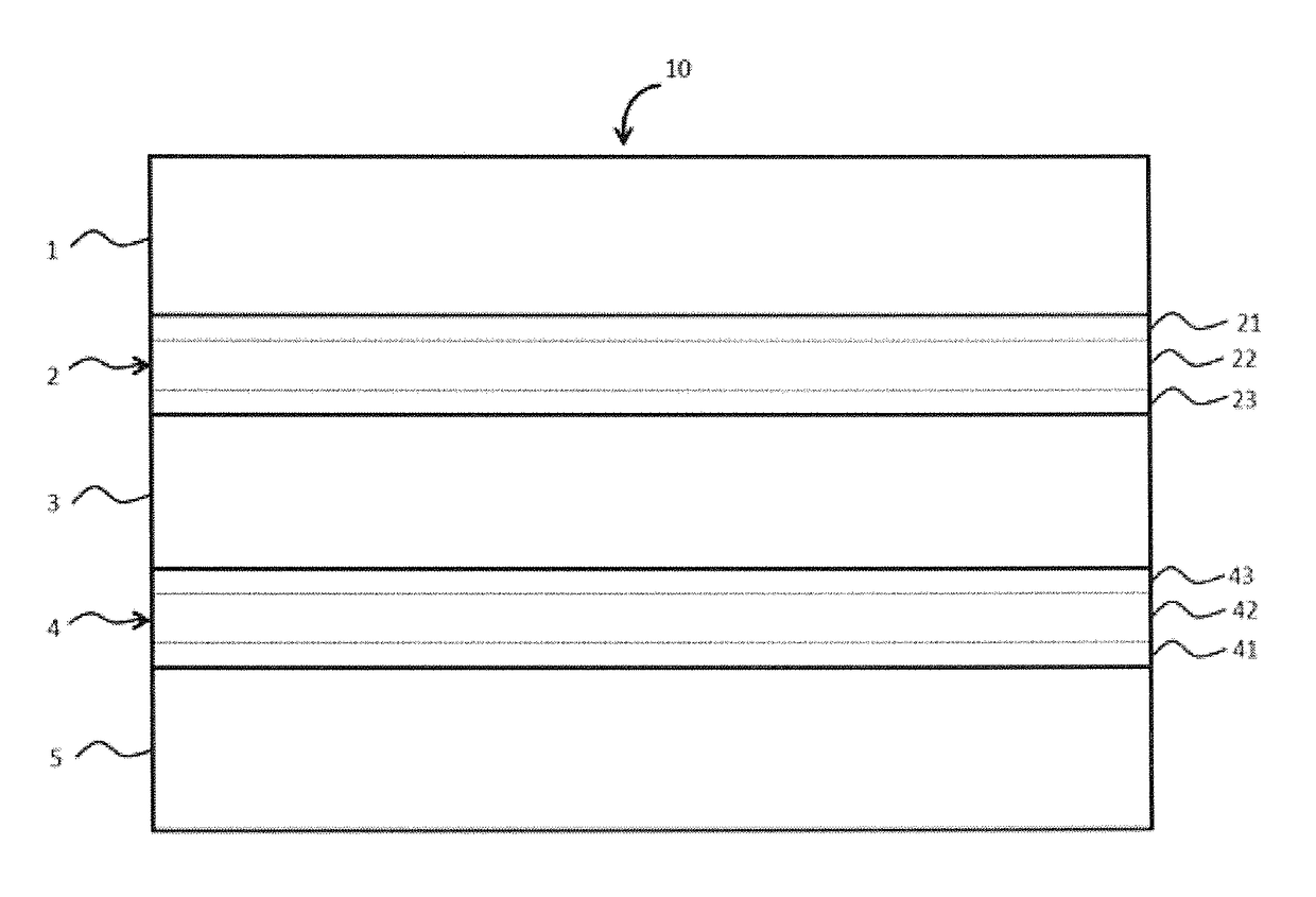
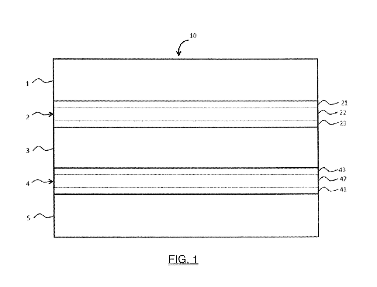
[0106]Films (S1-S4) were prepared with a first (outer) layer of 46 μm, a second (inner) layer of 368 μm and a third (outer) layer of 46 μm. The films were processed at 120° C. After production, films were stored in Aluminum-lined sealed bags. The two outer layers (1 and 3) comprise Yparex 1 prepared according to example 1. The inner layer (2) is varied.

[0107]The films were laminated between glass and a backsheet (25 minutes cycle, of which 18 minutes at 155° C.). The adhesion of the four different polymeric materials on the backsheets AAA3554 and TPC3480 was tested. Also transmission and haze of the films have been determined. The results are shown in Table 3.

TABLE 3Peel strength afterPeel strengththermal cycle testdirectly after(100 cycles −40° C.Opticallaminationto 90° C.)propertiesPolymericCuPACuPATrans-Ex.Mater...


PUM

PropertyMeasurementUnit
densityaaaaaaaaaa
vol %aaaaaaaaaa
vol %aaaaaaaaaa

Abstract

An electronic device module including a glass cover sheet, a polymeric front polymeric material, an electronic device, a polymeric back material and a backsheet, wherein the polymeric front and / or back materials have a trilayer structure including a back layer which is adhered to a surface of the electronic device, a front layer which is adhered to the glass cover sheet or the backsheet and an intermediate layer between the back layer and the front layer, wherein each of the back layer and the front layer includes an ethylene interpolymer grafted with silane, wherein the ethylene interpolymer grafted with silane has a density of at most 0.905 g / cm3, and the intermediate layer is a non-grafted ethylene interpolymer having a density of at most 0.905 g / cm3, which is crosslinked with the aid of a crosslinking initiator and optionally a crosslinking coagent, and optionally additives. A trilayer polymeric film having outer layers including ethylene interpolymers grafted with silanes and a non-grafted innerlayer containing a peroxide and UV stabilizer.

Description

FIELD OF THE INVENTION[0001]The invention relates to electronic device modules. In particular, the invention relates to electronic device modules comprising an electronic device, e.g., a solar or photovoltaic (PV) cell and a protective polymeric material.BACKGROUND OF THE INVENTION[0002]Polymeric materials are commonly used in the manufacture of modules comprising one or more electronic devices including, but not limited to, solar cells (also known as photovoltaic cells), liquid crystal panels, electro-luminescent devices and plasma display units. The modules often comprise an electronic device in combination with one or more substrates, e.g., one or more glass cover sheets, often positioned between two substrates in which one or both of the substrates comprise glass, metal, plastic, rubber or another material. The polymeric materials are typically used as the encapsulant for the module or, depending upon the design of the module, as a skin layer component of the module, e.g. a back...

Claims


Application Information

Patent Timeline
Patent Type & Authority Applications(United States)
IPC IPC(8): H01L31/048B29C47/06B32B27/32B32B17/10B29C47/00B29C48/21B29C48/92B29L7/00B29L9/00
CPCH01L31/0481B29C47/065B29C47/0004B32B27/327B32B17/10018B32B2457/12B29K2023/04B29L2007/008B29L2009/00B32B2307/412B32B17/1055B29C48/92B29C48/07B29C48/21B32B27/32B32B37/153H01L31/048B29C2948/92704Y02E10/50B32B2315/08B32B17/10688B29C48/022
Inventor KUIJK, EGBERT WILLEMBIJLEVELD, ERIK CORNELIS
Owner YPAREX BV
Why Eureka
Try Eureka