Tunneling transistor and method of fabricating the same
- Summary
- Abstract
- Description
- Claims
- Application Information
AI Technical Summary
Benefits of technology
Problems solved by technology
Method used
Image

Examples
Embodiment Construction
[0021]To provide a better understanding of the present invention, preferred embodiments will be described in detail. The preferred embodiments of the present invention are illustrated in the accompanying drawings with numbered elements.
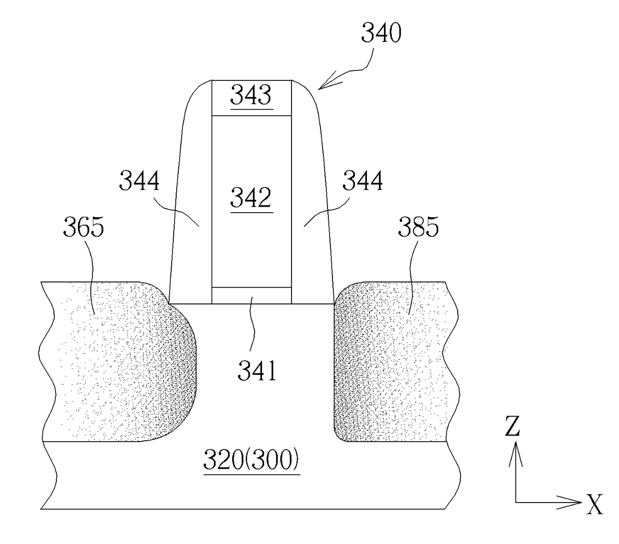
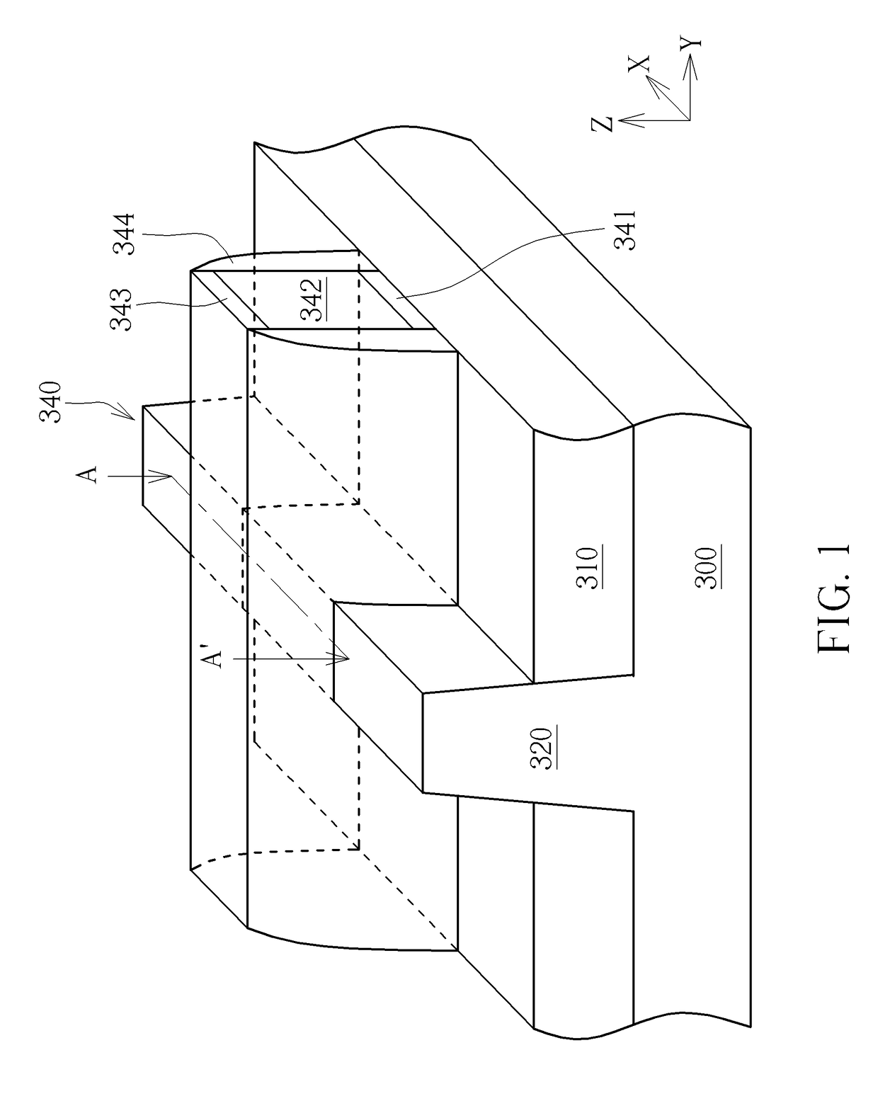
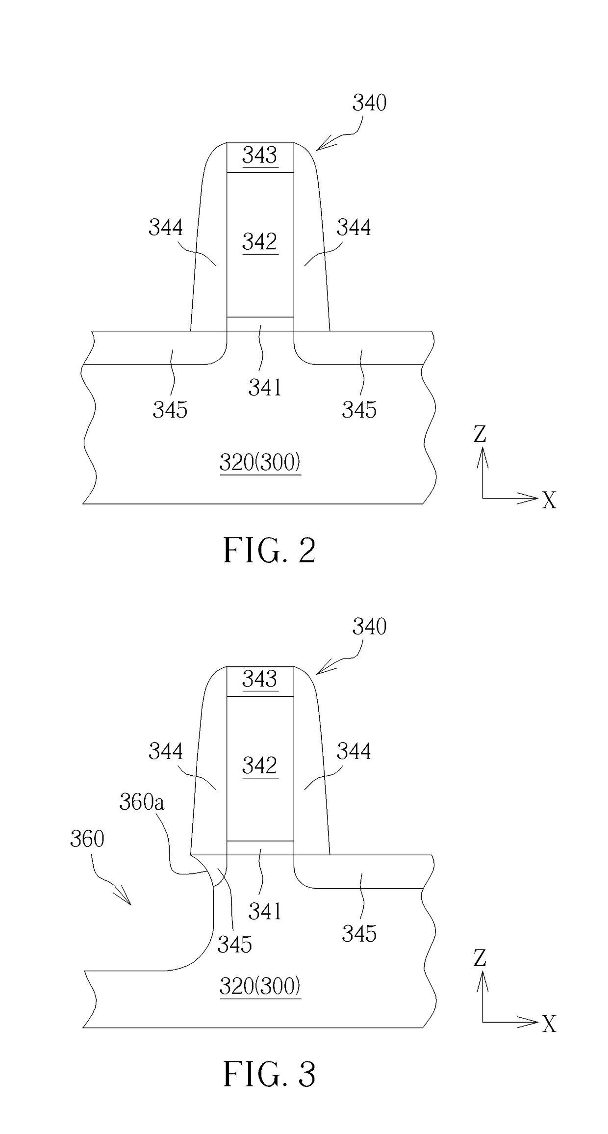
[0022]Referring to FIGS. 1-7, FIGS. 1-7 illustrate a fabricating method of a tunneling transistor according to the first preferred embodiment of the present invention. As shown in FIGS. 1-2, a substrate 300 for example a bulk silicon substrate, an epitaxial silicon substrate or a silicon-on-insulator (SOI) substrate is firstly provided. Then, at least one fin shaped structure 320 is formed in the substrate 300 and at least one gate structure 340 is formed across the fin shaped structure 320. It should be noted that the quantity of the fin shaped structure 320 and the gate structure 340 is not limited to what is shown in FIG. 2 and more fin shaped structure 320 and more gate structure 340 may be formed depended on the practical requirements.
[0023]For e...
PUM
 Abstract
Description
Claims
Application Information
 - Generate Ideas
- Intellectual Property
- Life Sciences
- Materials
- Tech Scout
- Unparalleled Data Quality
- Higher Quality Content
- 60% Fewer Hallucinations
Browse by: Latest US Patents, China's latest patents, Technical Efficacy Thesaurus, Application Domain, Technology Topic, Popular Technical Reports.
© 2025 PatSnap. All rights reserved.Legal|Privacy policy|Modern Slavery Act Transparency Statement|Sitemap|About US| Contact US: help@patsnap.com