Optical modulation device

a modulation device and optical technology, applied in the field of optical modulation devices, can solve the problems of reducing the characteristic impedance accuracy of a narrow width signal line, affecting the propagation speed of electrical signals, and affecting the accuracy of forming signal lines with greatly different characteristics, so as to achieve the effect of reducing the width of the signal line, increasing the characteristic impedance, and high adjustment accuracy of the impedan

Inactive Publication Date: 2018-02-08
SUMITOMO ELECTRIC IND LTD
View PDF12 Cites 6 Cited by
  • Summary
  • Abstract
  • Description
  • Claims
  • Application Information

AI Technical Summary

Benefits of technology

[0005]In a case where a signal line is branched three times into signal lines on a micro strip substrate, when input impedance of a signal fed into the micro strip substrate is, for example, 50Ω (ohms), it is necessary to enlarge characteristic impedance of the branched signal lines to 100Ω, 200Ω and 400Ω in order to achieve impedance matching. However, it is difficult to form signal lines that have characteristic impedance greatly different from each other, on a single micro strip substrate. The width of the signal line may be reduced in order to increase characteristic impedance, but the accuracy of the characteristic impedance of a narrow width signal line may be d...

Problems solved by technology

However, it is difficult to form signal lines that have characteristic impedance greatly different from each other, on a single micro strip substrate.
The width of the signal line may be reduced in order to increase characteristic impedance, but the accuracy of the characteristic impedance of a narrow width signal line may be degraded because of a limitation of forming accuracy of the width.
Thereby, there is variability in propagation loss and ...

Method used


Image

  • Optical modulation device
  • Optical modulation device
  • Optical modulation device

Examples


first embodiment

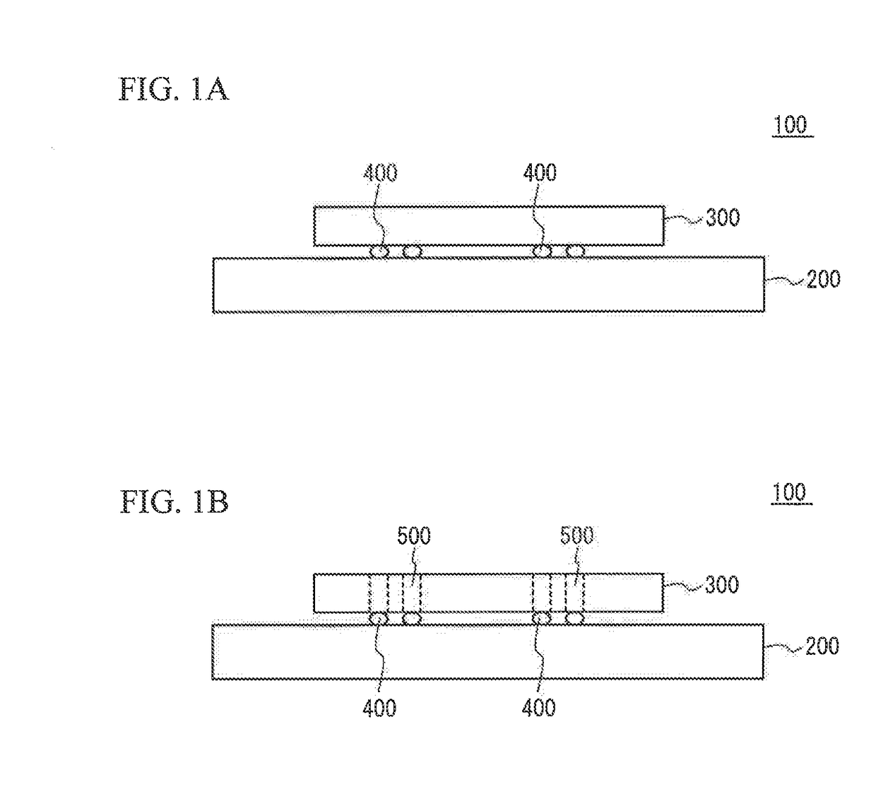
[0039]FIG. 1A and FIG. 1B illustrate a schematic side views of an optical modulation device 100 in accordance with a first embodiment. As illustrated in FIG. 1A, the optical modulation device 100 has a structure in which a driver chip 300 is mounted on an upper face of a modulator chip 200 through a bump 400. In FIG. 1A, the upper face of the modulator chip 200 is a face for forming elements. A lower face of the driver chip 300 (a face facing the modulator chip 200) is a face for forming elements. The face for forming elements of the modulator chip 200 is electrically coupled with the face for forming elements of the driver chip 300 via the bump 400. When the face for forming elements of the driver chip 300 is opposite to the modulator chip 200, a through-hole conductive via 500 may be formed in the driver chip 300, as illustrated in FIG. 1B. The face for forming elements of the modulator chip 200 is electrically coupled with the face for forming elements of the driver chip 300 via ...

first modified embodiment

[0068]A delay amount may be adjusted by providing a variable capacitance diode in at least one of the first signal transmission line 305 and the second signal transmission line 306. FIG. 11A and FIG. 11B illustrate another example of the first signal transmission line 305 and the second signal transmission line 306. FIG. 11A illustrates a plan view of the first signal transmission line 305 and the second signal transmission line 306. FIG. 11B illustrates a cross sectional view taken along a line E-E of FIG. 11A. As illustrated in FIG. 11A and FIG. 11B, the ground electrode 52 has an opening below the transmission line 51. The transmission line 51 passes through the opening and penetrates the fourth insulation layer 48, the third interconnection layer 47, the third insulation layer 46, the second interconnection layer 45, the second insulation layer 44, the first interconnection layer 43 and the first insulation layer 42, and is coupled with an one end of the variable capacitance dio...

second modified embodiment

[0073]When it is difficult to adjust delay matching between an optical signal and an electrical signal only by the first signal transmission line 305 and the second signal transmission line 306, the delay matching may be adjusted by changing the lengths of the arm waveguides 13a and 13b. For example, as illustrated in FIG. 12, the delay amount may be adjusted by providing a curved portion in the arm waveguides 13a and 13b between the phase modulator 21 and the phase modulator 22.


PUM


Abstract

An optical modulation device includes: a Mach-Zehnder modulator including a semiconductor waveguide; a plurality of phase modulators that are spaced from each other; a first amplifier that is coupled with an input transmission line transmitting an electrical signal, has an input impedance substantially equal to a characteristic impedance of the input transmission line; a first interconnection that is coupled to the first amplifier and transmits the electrical signal to a first end of one of the plurality of phase modulators that is provided on an input side of the Mach-Zehnder modulator; a second interconnection that is coupled to the first amplifier and transmits the electrical signal to a first end of the other of the plurality of phase modulators that is provided on an output side of the Mach-Zehnder modulator; and a plurality of termination resistors respectively coupled to second ends of the plurality of phase modulators.

Description

CROSS-REFERENCE TO RELATED APPLICATION[0001]This application is based upon and claims the benefit of priority of the prior Japanese Patent Application No. 2016-155857, filed on Aug. 8, 2016, the entire contents of which are incorporated herein by reference.BACKGROUND(i) Technical Field[0002]The present invention relates to an optical modulation device.(ii) Related Art[0003]As a device for modulating a light in accordance with an input high speed electrical signal, there is known a Mach-Zehnder modulator that has a transmission line type electrode and has a termination resistor at an end of the electrode, the termination resistor being terminated with a resistance equal to characteristic impedance of the electrode.[0004]For example, there are disclosed a LiNbO3 type Mach-Zehnder modulator that has a transmission line type electrode on an arm and a micro strip substrate that divides one input signal to a plurality of paths and has a driver amplifier on each path (for example, see U.S....

Claims


Application Information

Patent Timeline
IPC IPC(8): G02F1/225H04B10/516G02B26/08G02F1/01G02F1/017
CPCG02F1/2255G02F1/0121G02F1/017G02B26/0841H04B10/5161G02F2203/50G02F1/225G02F2201/16G02F1/212H01S3/00
Inventor FURUYA, AKIRATATSUMI, TAIZO
Owner SUMITOMO ELECTRIC IND LTD
Why Eureka
Try Eureka