Sputtering apparatus

Inactive Publication Date: 2018-03-01
ULVAC INC
View PDF3 Cites 1 Cited by
  • Summary
  • Abstract
  • Description
  • Claims
  • Application Information

AI Technical Summary

Benefits of technology

This patent describes a sputtering apparatus for improving the quality of insulator films in semiconductor devices. The apparatus includes a gettering metal target and a DC power source for sputtering a second target. The gettering effect helps to quickly reduce the pressure in the vacuum chamber, resulting in a higher quality insulator film with improved crystallinity. To prevent contamination between the targets, a shielding means is used to selectively shield the surfaces of the targets facing the substrate. The technical effects of this invention are improved quality and productivity of insulator films in semiconductor devices.

Problems solved by technology

The annealing temperature has limitations from the viewpoint of limitations of the apparatus, and limitations due to the film arrangement of primary layers, and the like and, as a consequence, the temperature can only be raised up to about 700° C. Therefore, when a magnesium oxide film is formed by using the sputtering apparatus, the crystallinity thereof is improved so that a still larger MR ratio can be expected to be attained.

Method used


Image

  • Sputtering apparatus
  • Sputtering apparatus
  • Sputtering apparatus

Examples


Embodiment Construction

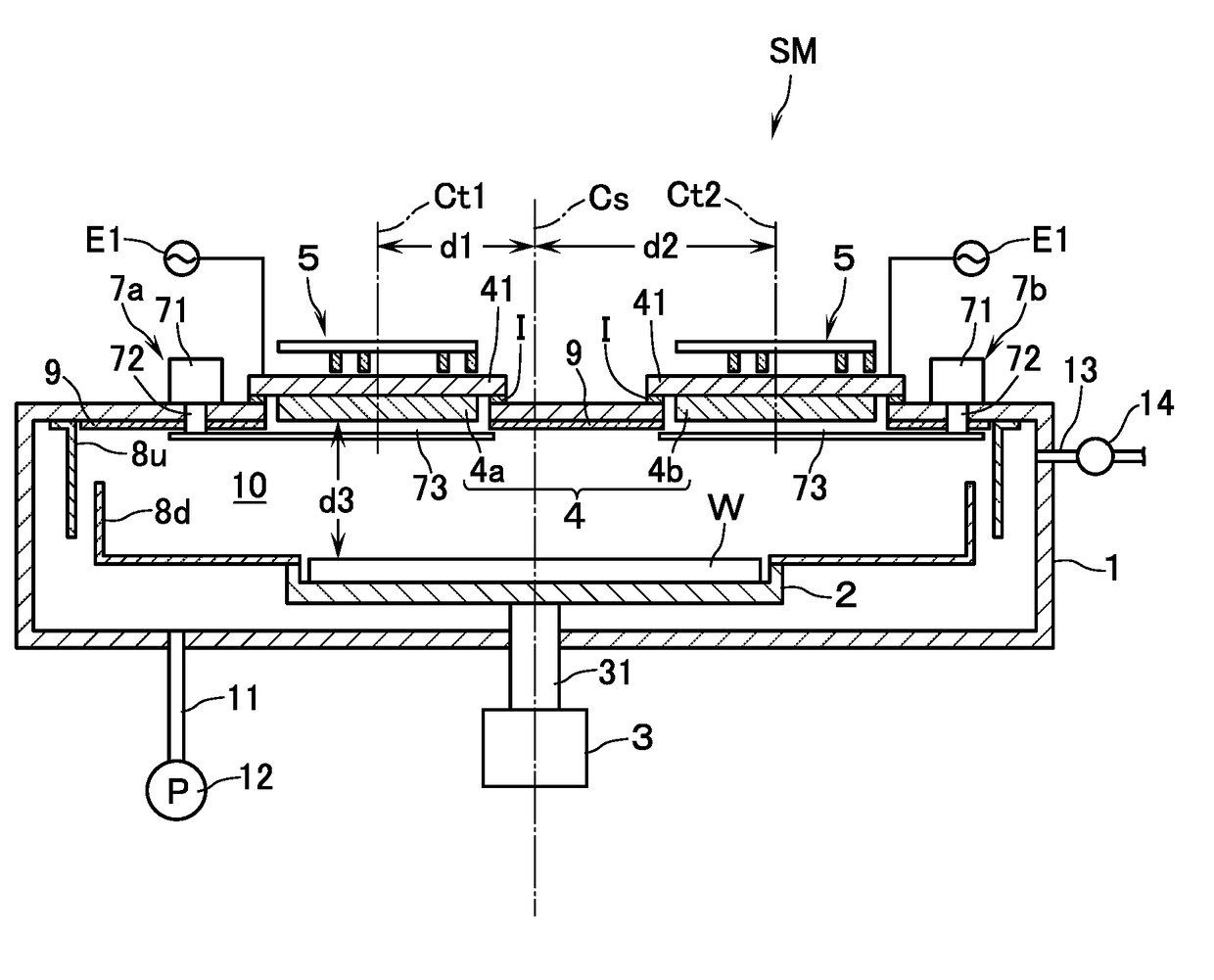
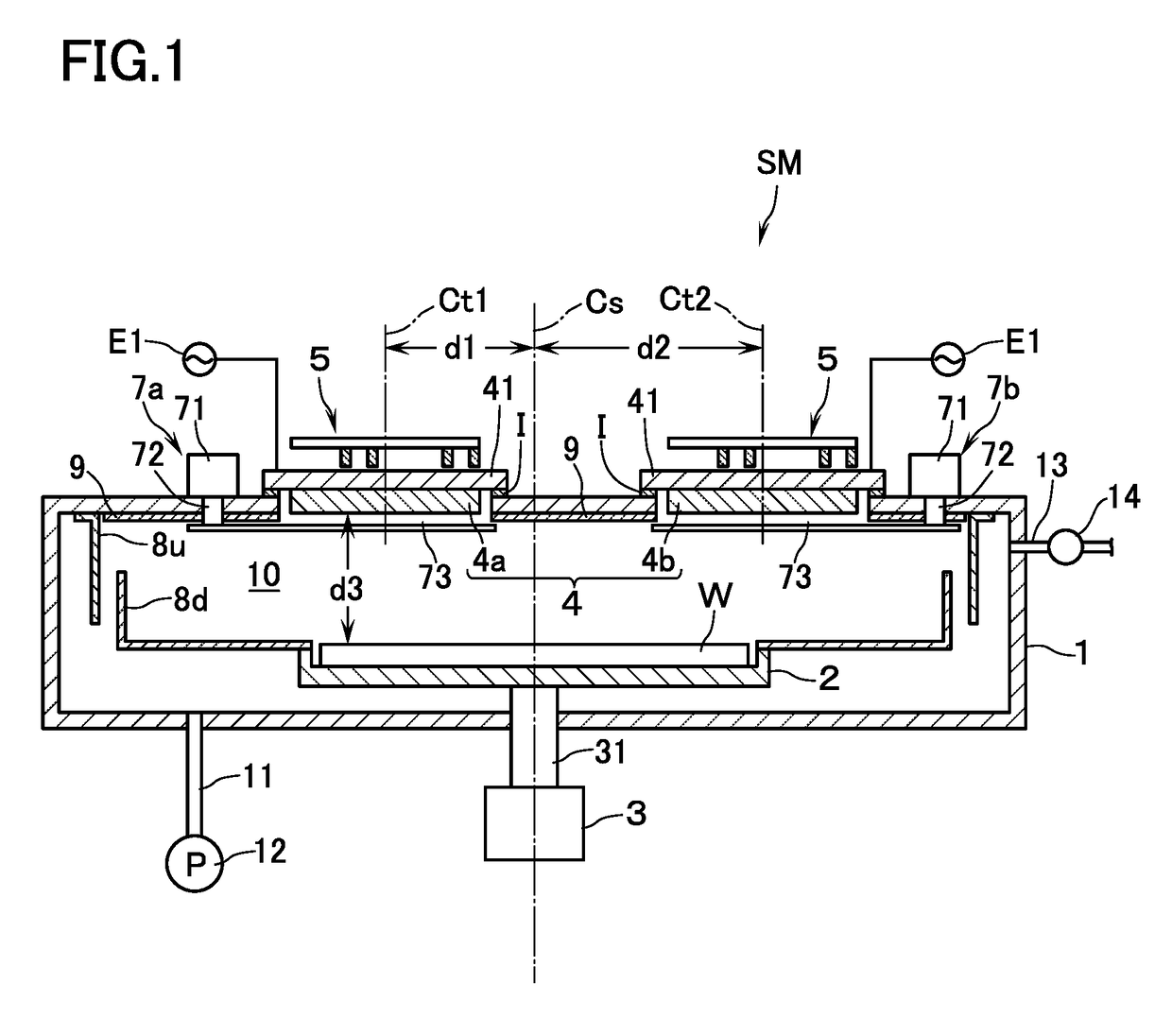
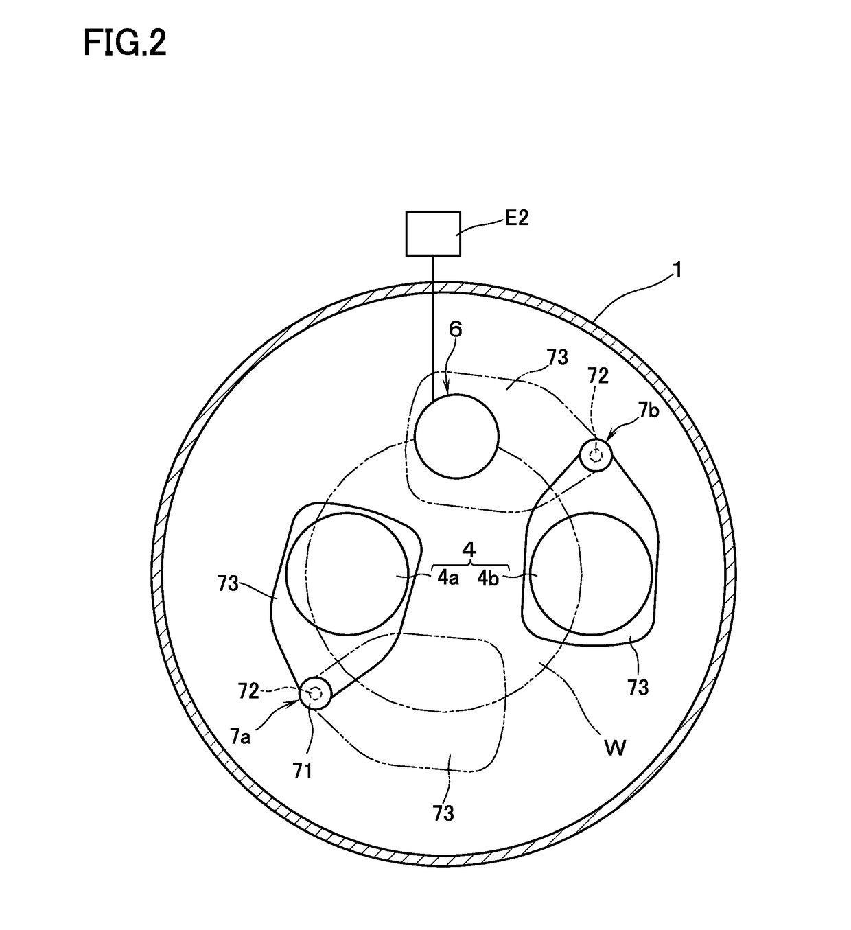
[0016]With reference to the accompanying drawings, a description will now be made of an embodiment of the sputtering apparatus of this invention on the basis of an example: in which a substrate W is supposed to be a silicon wafer of 300 mm (in diameter); and in which an insulator target 4 is supposed to be a target made of magnesium oxide so that a magnesium oxide film as an insulator film is formed on the surface of the substrate. In the following, a description will be made by referring to FIG. 1 for the meaning of the terms indicating the directions, such as “upper” and “lower.”

[0017]With reference to FIG. 1, reference characters SM refer to a sputtering apparatus according to this embodiment. The sputtering apparatus SM is provided with a vacuum chamber 1 which defines a processing chamber 10. To a bottom wall of the vacuum chamber 1, there is connected, through an exhaust pipe 11, a vacuum pump 12 so that the vacuum chamber 1 can be evacuated to a predetermined pressure (e.g., ...


PUM

PropertyMeasurementUnit
Crystallinityaaaaaaaaaa
Areaaaaaaaaaaa
Distanceaaaaaaaaaa

Abstract

There is provided a sputtering apparatus which is capable of forming, with good uniformity of film thickness distribution, an insulator film having further improved crystallinity. Inside a vacuum chamber in which is provided an insulator target, there is disposed a stage for holding a substrate W to be processed so as to face the insulator target. The sputtering apparatus has: a driving means for driving to rotate the stage; a sputtering power source E1 for applying HF power to the insulator target; and a gas introduction means for introducing a rage gas into the vacuum chamber. The sputtering apparatus is characterized in that a distance d3 between the substrate and the insulator target is set to a range between 40 mm-150 mm.

Description

TECHNICAL FIELD[0001]The present invention relates to a sputtering apparatus for forming a film made of an insulating material such as magnesium oxide film and the like.BACKGROUND ART[0002]Attention has recently been paid to a Magnetic Random Access Memory (MRAM) which employs Magnetic Tunnel Junction (MTJ) elements by utilizing Tunneling Magneto Resistance (TMR) effect. Then, as such a tunnel barrier layer of the MTJ elements as is made by sandwiching the tunnel barrier layer by means of electrode layers of two ferromagnetic materials, it is being contemplated to use crystalline magnesium oxide (MgO) films. In order to improve the properties of this kind of MTJ elements, one of the important elements is the rate of change in magnetic resistance (rate of change: MR ratio between the tunnel resistance (RP) when the magnetization of electrode layers on both sides is parallel with each other, and the tunnel resistance (RAP) when the magnetization of electrode layers on both sides is an...

Claims


Application Information

Patent Timeline
IPC IPC(8): C23C14/34H01L43/12H01J37/34C23C14/50C23C14/56
CPCC23C14/34H01L43/12H01J37/3417H01J37/3426H01J37/345C23C14/50C23C14/566C23C14/082C23C14/081C23C14/352H01J37/3405H01J37/3447H01J37/3473H10N50/01C23C14/3414C23C14/505C23C14/54C23C14/3464C23C14/564
Inventor YAMAMOTO, HIROKINANBA, TAKAHIROKAMII, MASANOBUKOHARI, SHINJIKONDO, TOMOYASUMORIMOTO, NAOKI
Owner ULVAC INC
Why Eureka
Try Eureka