Photoelectric conversion device
- Summary
- Abstract
- Description
- Claims
- Application Information
AI Technical Summary
Benefits of technology
Problems solved by technology
Method used
Image

Examples
examples
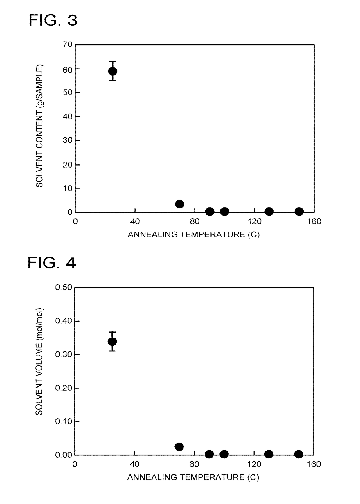
[0063]Next, examples and evaluation results thereof will be described.
examples 1 to 4
, Comparative Examples 1 to 3
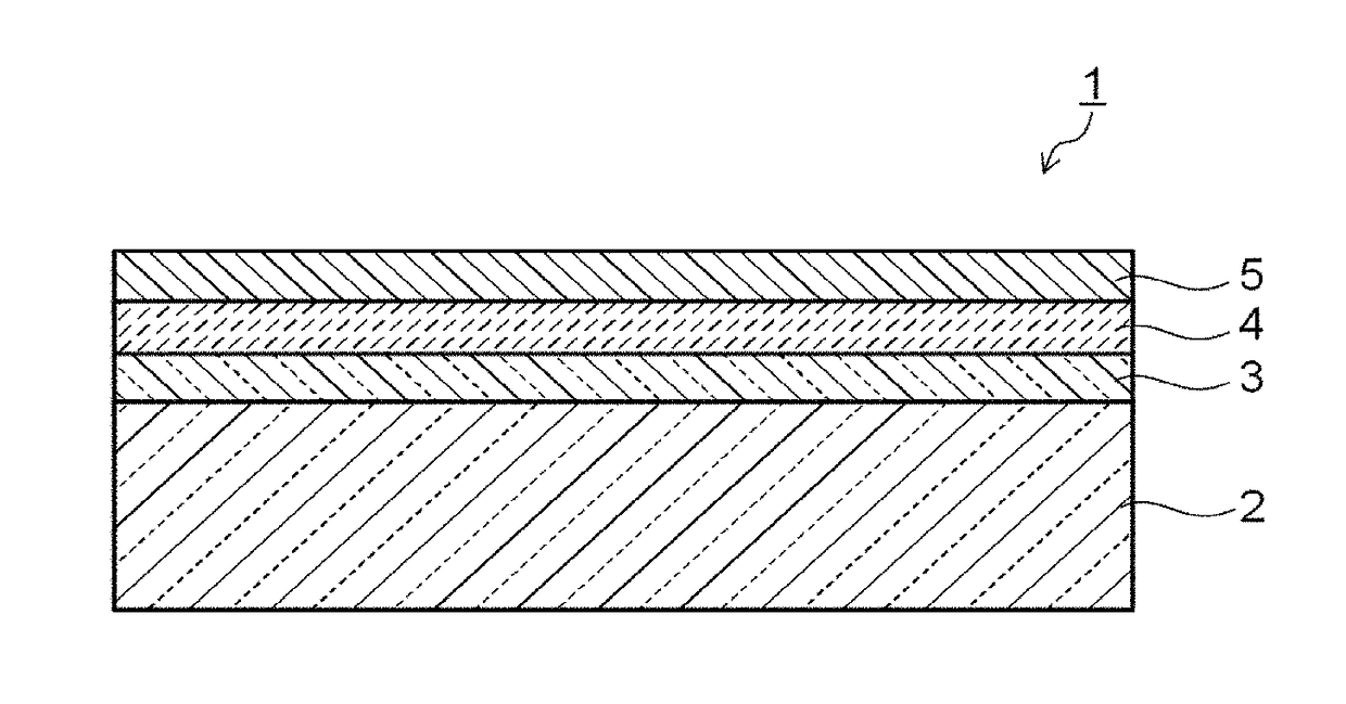
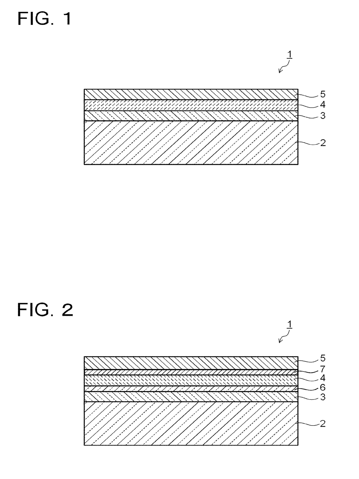
Production of Photoelectric Conversion Device
[0064]After forming an ITO film as a first electrode on a glass substrate, ultrasonic cleaning and UV cleaning were performed in isopropyl alcohol and acetone. A base layer with a thickness of about 50 nm, which contained PEDOT:PSS, was formed on the glass substrate having the ITO film. The PEDOT:PSS layer functions as a hole transport layer. The PEDOT:PSS layer was formed by applying HIL1.1 (product name, made by Heraeus Holding GmbH) at 5000 rpm, thereafter drying it at 140° C. for ten minutes.
[0065]Next, a perovskite crystal layer was film-formed as a photoelectric conversion layer as follows. First, a perovskite material solution (coating solution) was prepared by dissolving methylammonium iodide (CH3NH3I) and lead iodide (PbI2) in N,N-dimethylformamide (DMF). The coating solution was adjusted so that a concentration in the solution became 45 mass % with a molar ratio of methylammonium iodide and lead iodi...
PUM
| Property | Measurement | Unit |
|---|---|---|
| Angle | aaaaa | aaaaa |
| Angle | aaaaa | aaaaa |
| Diameter | aaaaa | aaaaa |
Abstract
Description
Claims
Application Information
 - R&D
- Intellectual Property
- Life Sciences
- Materials
- Tech Scout
- Unparalleled Data Quality
- Higher Quality Content
- 60% Fewer Hallucinations
Browse by: Latest US Patents, China's latest patents, Technical Efficacy Thesaurus, Application Domain, Technology Topic, Popular Technical Reports.
© 2025 PatSnap. All rights reserved.Legal|Privacy policy|Modern Slavery Act Transparency Statement|Sitemap|About US| Contact US: help@patsnap.com