Compound for organic electric element, organic electric element comprising the same and electronic device thereof

a technology of organic electric elements and organic electric elements, which is applied in the direction of organic chemistry, luminescent compositions, chemistry apparatus and processes, etc., can solve the problems of power consumption, efficiency and life span issues, and the need to increase the need for power consumption, so as to improve the planity of molecules, improve the ability of hole transport and thermal stability, and improve the effect of t1 valu

Active Publication Date: 2018-03-22
DUK SAN NEOLUX
View PDF3 Cites 10 Cited by
  • Summary
  • Abstract
  • Description
  • Claims
  • Application Information

AI Technical Summary

Benefits of technology

[0017]According to the embodiments of the present invention, by using a specific compound having a substituent which enhances the planity of a molecule as a material of the organic electric device, hole transport ability and thermal stability are improved, and the HOMO energy level and the high T1 value are easy to balance the charge in the light emitting layer. As a result, luminous efficiency, heat-resistance, and lifetime of the organic electric elements can be improved and a driving voltage of the organic electric elements can be lowered.

Problems solved by technology

Currently, the power consumption is required more and more as size of display becomes larger and larger in the portable display market.
Therefore, the power consumption is a very important factor in the portable display with a limited power source of the battery, and efficiency and life span issue also must be solved.
However, efficiency cannot be maximized only by simply improving the organic material layer.
As a result, the exciton generated in the light emitting layer is transferred to the hole transport layer, resulting in a charge unbalance in the light emitting layer and light is emitted at the interface of the hole transport layer.
However, this cannot be achieved simply by the structural properties of the core of an emission-auxiliary layer material.

Method used


Image

  • Compound for organic electric element, organic electric element comprising the same and electronic device thereof
  • Compound for organic electric element, organic electric element comprising the same and electronic device thereof
  • Compound for organic electric element, organic electric element comprising the same and electronic device thereof

Examples


synthesis example

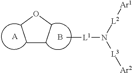
[0088]The compound (final products) represented by Formula 1 according to the present invention are synthesized by reacting Sub 1 and Sub 2 as shown in Reaction Scheme 1, but are not limited thereto.

[0089]A ring, B ring, L1 to L3, Ar1 and Ar2 are each identical as defined in formula 1 above.

[0090]I. Synthesis of Sub 1

[0091]Sub 1 of the Reaction Scheme 1 can be synthesized according to, but not limited to, the reaction route of the following Reaction Scheme 2.

[0092]Synthesis Examples of compounds comprised in Sub 1 are as follows.

1. Synthesis Example of Sub 1-3

[0093]

(1) Synthesis of Sub 1-I-3

[0094]The starting material 2-(4-bromophenyl)naphthalen-1-ol (29.89 g, 99.91 mmol) was placed into a round bottom flask together with Pd(OAc)2 (2.24 g, 9.99 mmol), 3-nitropyridine (1.24 g, 9.99 mmol), then, dissolved in C6F6 (150 ml) and DMI (100 ml). And then, tert-butyl peroxybenzoate (38.81 g, 199.83 mmol) was added, and stirred 90° C. When the reaction was completed, the reaction product was ...

example i-2

[Example I-2] to [Example I-34] Green OLED (A Hole Transport Layer)

[0184]The OLEDs were fabricated in the same manner as described in Example I-1 except that the compounds P-3 to P-48 of the present invention described in Table 4 instead of the compound P-1 of the present invention were used as the hole transport layer material.

[Comparative Example I-1] to [Comparative Example I-8]

[0185]The OLEDs were fabricated in the same manner as described in Example 1 except that the following Comparative Compounds 1 to 8 instead of the compound P-1 of the present invention were each used as the hole transport layer material.

[0186]Electroluminescence (EL) characteristics were measured with a PR-650 (Photoresearch) by applying a forward bias DC voltage to the OLEDs prepared in Examples I-1 to I-34 of the present invention and Comparative Examples I-1 to I-8. And, the T95 life time was measured using a life time measuring apparatus manufactured by Macscience Inc. at reference brightness of 5000 c...

example ii-1

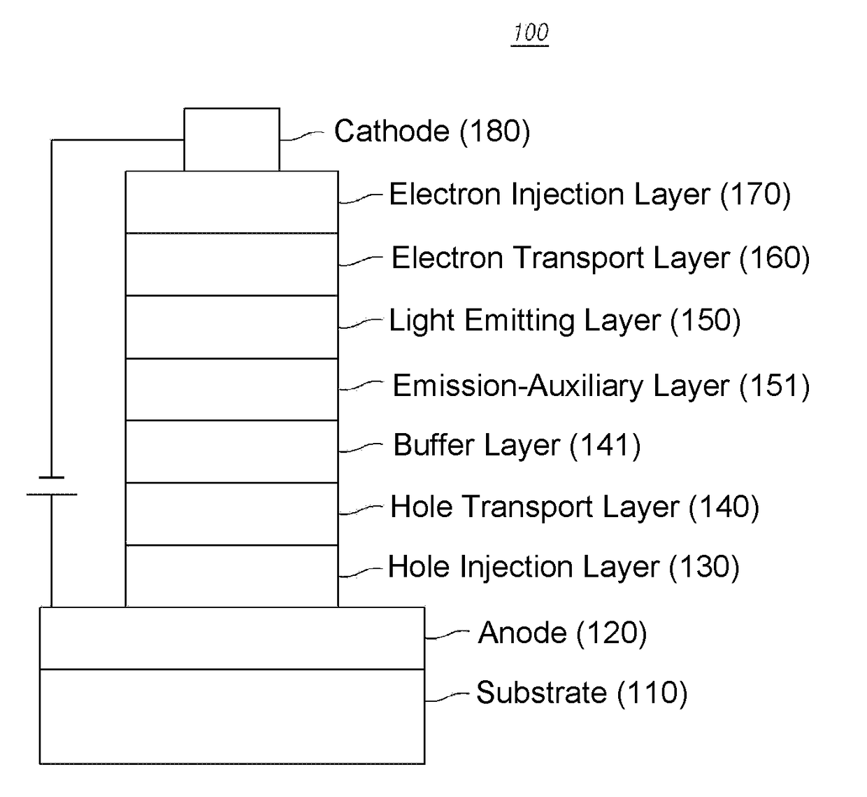
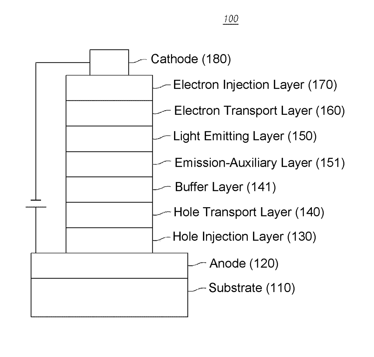
[Example II-1] Green OLED (an Emission-Auxiliary Layer)

[0196]Organic light emitting diodes (OLEDs) were fabricated according to a conventional method by using a compound of the present invention as an emission-auxiliary layer material.

[0197]First, an ITO layer (anode) was formed on a glass substrate, and a film of 2-TNATA was vacuum-deposited on the ITO layer to form a hole injection layer with a thickness of 60 nm. Subsequently, Comparative compound 1 was vacuum-deposited with a thickness of 60 nm on the hole injection layer to form a hole transport layer.

[0198]Subsequently, a film of the compound P-1 of the present invention was vacuum-deposited on the hole transport layer to form a emission-auxiliary layer with a thickness of 20 nm. A light emitting layer with a thickness of 30 nm was deposited on the emission-auxiliary layer by using the CBP as a host material and Ir(ppy)3 as a dopant material in a weight ratio of 90:10.

[0199]Next, a film of BAlq was vacuum-deposited with a thic...


PUM

PropertyMeasurementUnit
thicknessaaaaaaaaaa
thicknessaaaaaaaaaa
thicknessaaaaaaaaaa

Abstract

Provided are a compound represented by Formula 1, and an organic electric element comprising a first electrode, a second electrode, and an organic material layer formed between the first electrode and the second electrode, wherein the organic material layer comprised the compound represented by Formula 1, and the driving voltage of an organic electronic device can be lowered, and the luminous efficiency, color purity and life time of an organic electronic device can be improved by comprising the compound represented by Formula 1 in the organic material layer.

Description

CROSS-REFERENCE TO RELATED APPLICATION[0001]This patent application claims priority from and the benefit under 35 U.S.C. 119(a) of Korean Patent Application No. 10-2015-0073550, filed on May 27, 2015, which is hereby incorporated by reference for all purposes as if fully set forth herein. Further, this application claims the benefit of priority in countries other than U.S.A, which is hereby incorporated by reference herein.BACKGROUNDTechnical Field[0002]The present invention relates to compounds for organic electric elements, organic electric elements comprising the same, and electronic devices thereof.Background Art[0003]In general, an organic light emitting phenomenon refers to a phenomenon in which electric energy is converted into light energy of an organic material. An organic electric element utilizing the organic light emitting phenomenon usually has a structure including an anode, a cathode, and an organic material layer interposed therebetween. In many cases, the organic ma...

Claims


Application Information

Patent Timeline
Patent Type & Authority Applications(United States)
IPC IPC(8): H01L51/00C07D307/77C07F7/08C07D409/04C09K11/06
CPCH01L51/0061C07D307/77H01L51/006C07F7/0812H01L51/0094C07D409/04C09K11/06H01L51/5088H01L51/5056H01L51/5012H01L51/5072H01L51/5092H01L51/0003H01L51/0004H01L51/0005H01L51/0073H01L51/0052H01L51/0058H01L51/0074C09K2211/1018C09K2211/1014C09K2211/1011C09K2211/1007C09K2211/1088H10K85/622H10K85/615H10K85/631H10K85/633H10K85/6574H10K50/00C07D307/91H10K85/636H10K85/40H10K50/11H10K50/15H10K50/16H10K50/17H10K50/18H10K50/171H10K71/12H10K71/13H10K71/135H10K85/626H10K85/6576
Inventor PARK, JUNG CHEOLCHOI, YEON HEELEE, MUN JAEMUN, SOUNG YUNKIM, KI WONPARK, NAMJINLEE, JUNG WOOK
Owner DUK SAN NEOLUX
Why Eureka
Try Eureka