Electronic component
a technology of electronic components and components, applied in the field of electronic components, can solve the problems of reducing the mechanical strength of the element body part, allowing cracks, etc., to generate easily, and achieve the effect of high q-value and easy generation
- Summary
- Abstract
- Description
- Claims
- Application Information
AI Technical Summary
Benefits of technology
Problems solved by technology
Method used
Image
Examples
example 1
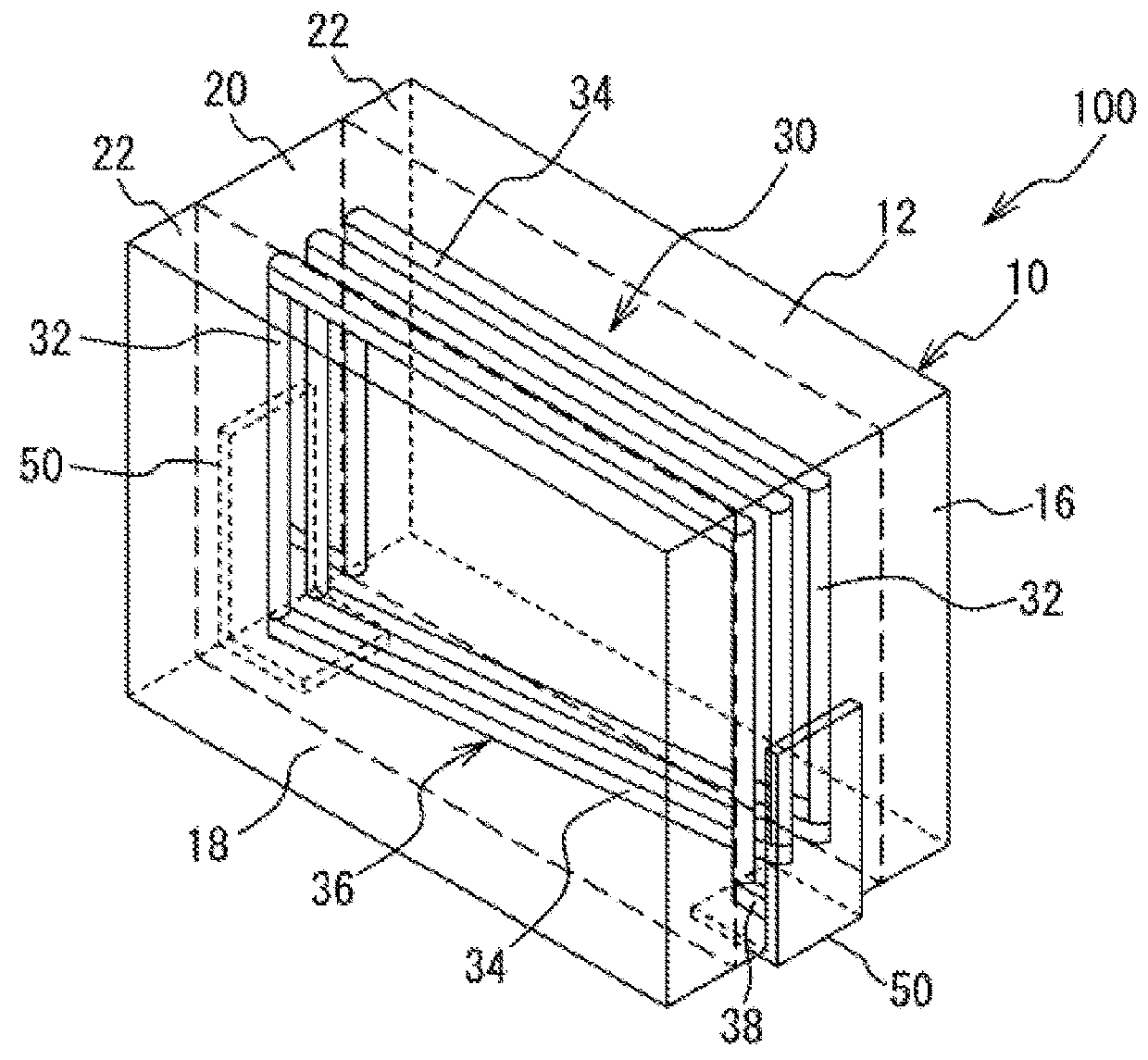
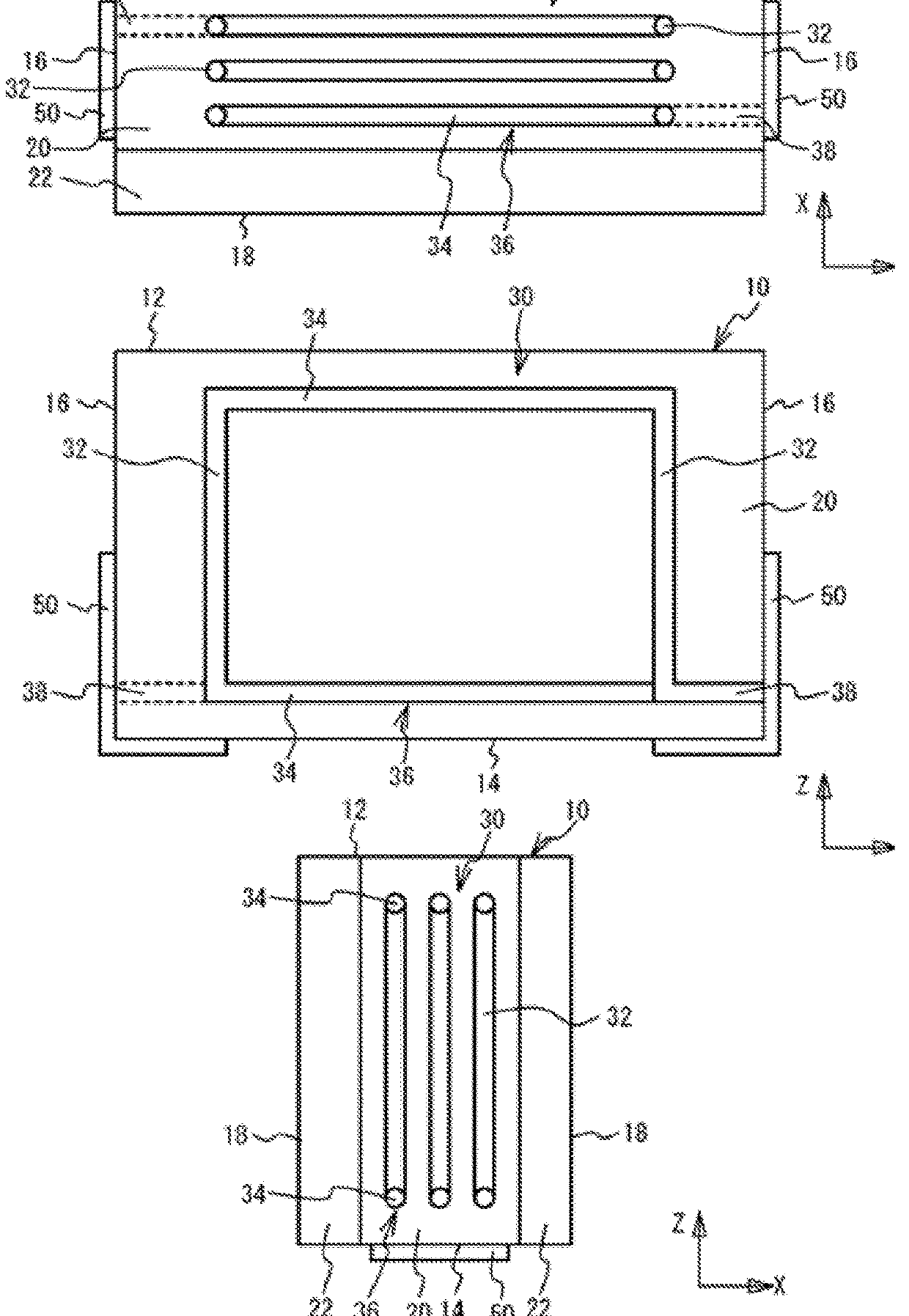
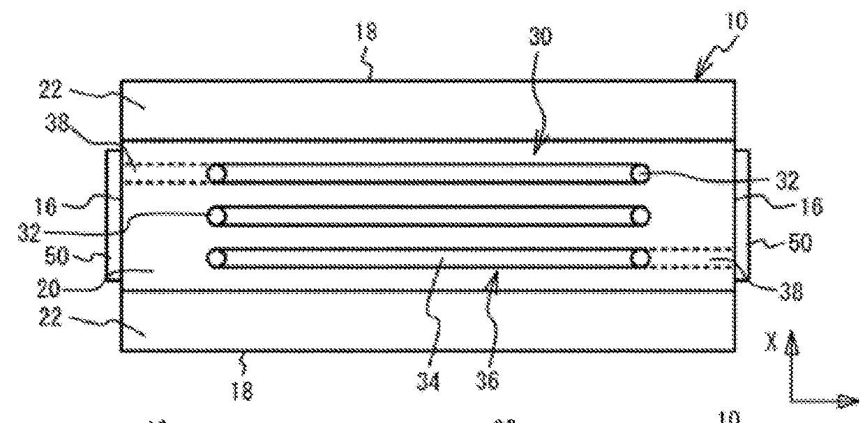
[0072]FIG. 1 is an oblique perspective view of the electronic component pertaining to Example 1. FIG. 2A is a top cross-sectional view, FIG. 2B is a side cross-sectional view, and FIG. 2C is an end cross-sectional view, of the electronic component pertaining to Example 1. As shown in FIG. 1 to FIG. 2C, the electronic component 100 in Example 1 comprises an element body part 10 constituted by an insulative body, an internal conductor 30, and external electrodes 50.
[0073]The element body part 10 has a top face 12 corresponding to a second face, a bottom face 14 corresponding to a first face, a pair of end faces 16, and a pair of side faces 18, and constitutes a rectangular solid shape having a width-direction side in the X-axis direction, a length-direction side in the Y-axis direction and a height-direction side in the Z-axis direction. The bottom face 14 represents a mounting surface, while the top face 12 is opposing the bottom face 14. The end faces 16 are each connected to a pair...
example 2
[0113]FIG. 8 is an oblique perspective view of the electronic component pertaining to Example 2. As shown in FIG. 8, an electronic component 200 in Example 2 is such that the high-hardness layer 22 is provided only on one side of the conductor-containing layer 20, while the part corresponding to the other side where the high-hardness layer 22 was provided in Example 1 is occupied by the conductor-containing layer 20. Other constitutions are the same as in Example 1 and therefore not explained.
[0114]The inventor conducted a deflection test on the electronic component in Example 2. The deflection test was conducted according to the same method explained in Example 1, and the dimensions of the electronic component, etc., were the same as in Example 1. Table 2 shows the deflection test results. It should be noted that the test results of Comparative Example 1 in Table 1 are also shown for the purpose of comparison.
TABLE 2DeflectionComparativeamountExample 2Example 1Number of cracks2 mm0...
example 3
[0117]FIG. 9 is an oblique perspective view of the electronic component pertaining to Example 3. It should be noted that, in FIG. 9, the internal conductor 30 has the same structure as in Example 1 and is therefore not illustrated in FIG. 9. As shown in FIG. 9, an electronic component 300 in Example 3 is such that external electrodes 50 are provided in a manner extending from the bottom face 14, via the end faces 16, to the top face 12, while also extending from the end faces 16, to the side faces 18, of the element body part 10. In other words, the external electrodes 50 cover the entire end faces 16, as well as parts of the top face 12, bottom face 14, and side faces 18. Other constitutions are the same as in Example 1 and therefore not explained.
[0118]The inventor conducted a deflection test on the electronic component in Example 3. The deflection test was conducted according to the same method explained in Example 1, and the dimensions of the electronic component, etc., were the...
PUM
| Property | Measurement | Unit |
|---|---|---|
| total thickness | aaaaa | aaaaa |
| total thickness | aaaaa | aaaaa |
| length | aaaaa | aaaaa |
Abstract
Description
Claims
Application Information


