Semiconductor device and semiconductor package

a semiconductor layer and semiconductor technology, applied in semiconductor devices, semiconductor/solid-state device details, diodes, etc., can solve the problems of difficult use of downsized semiconductor elements, and achieve the effects of reducing the concentration of impurity in the semiconductor layer, reducing the resistance per unit length, and reliable electric current cut o

Active Publication Date: 2018-04-05
ROHM CO LTD
View PDF8 Cites 16 Cited by
  • Summary
  • Abstract
  • Description
  • Claims
  • Application Information

AI Technical Summary

Benefits of technology

[0006]An electric current flowing through a semiconductor layer is cut off by a depletion layer expanding in the semiconductor layer upon application of a voltage. By properly designing expansion width of the depletion layer, reliable cut off of the electric current is secured. Therefore, with the JFET, the expansion width of the depletion layer has to be preferentially taken into consideration and impurity concentration (channel concentration) of the semiconductor layer is lowered. As a result, resistance per unit length is relatively high. There is also a depletion-mode MOSFET as the normally-on semiconductor element. However, for the same reason that expansion width of a depletion layer is preferentially taken into consideration, a decrease in resistance of a semiconductor layer is prevented.

Problems solved by technology

Therefore, it is difficult to downsize the semiconductor element for use.

Method used


Image

  • Semiconductor device and semiconductor package
  • Semiconductor device and semiconductor package
  • Semiconductor device and semiconductor package

Examples


Embodiment Construction

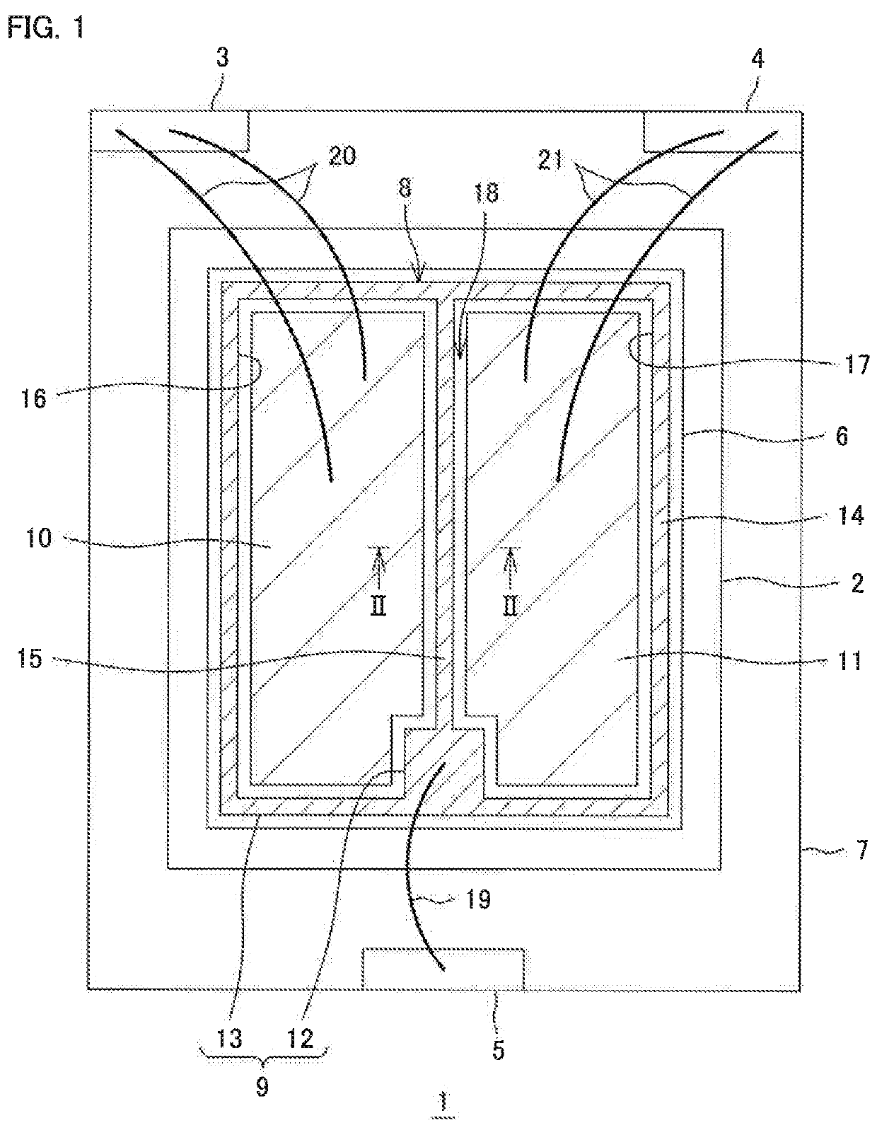
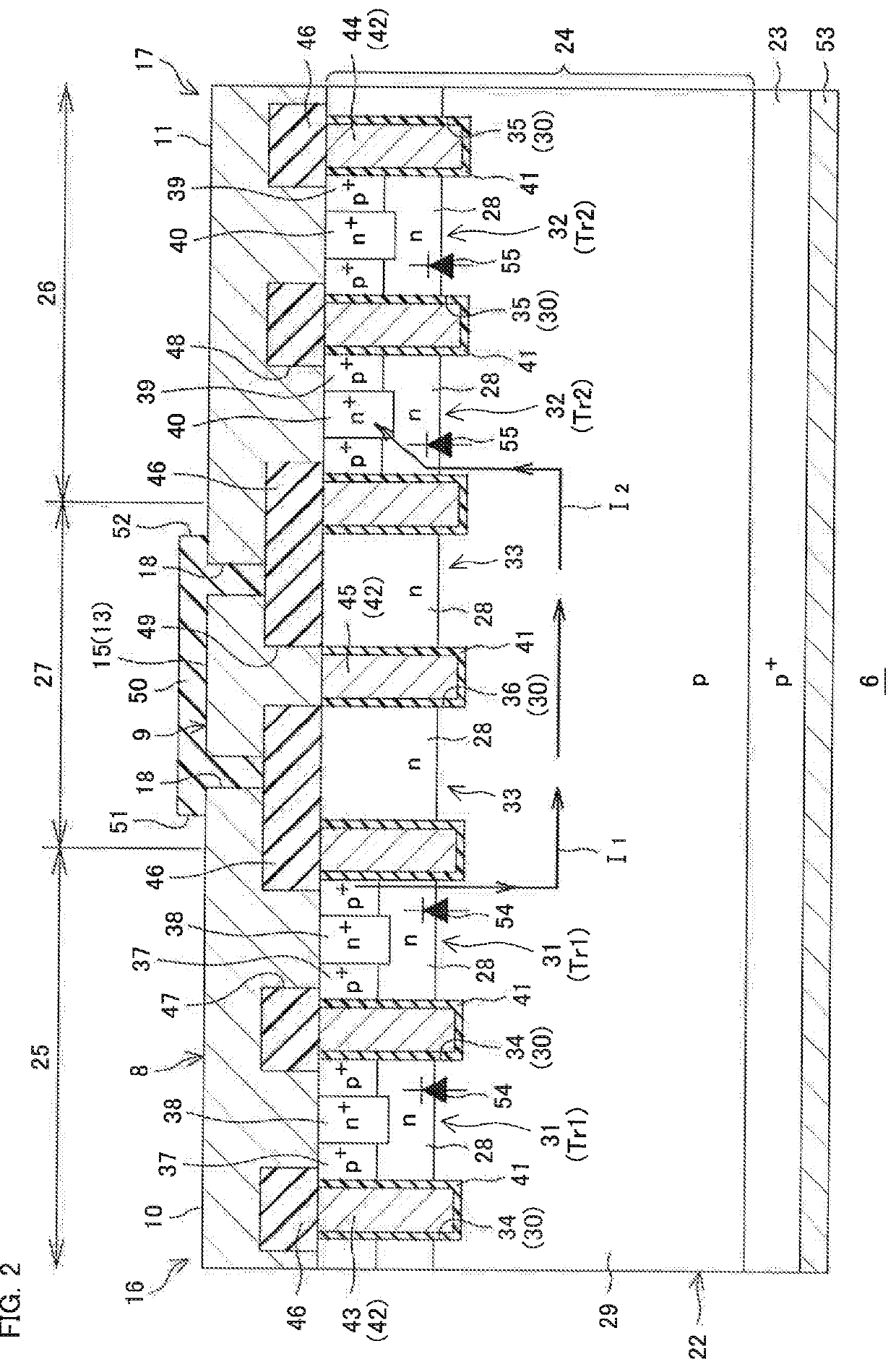
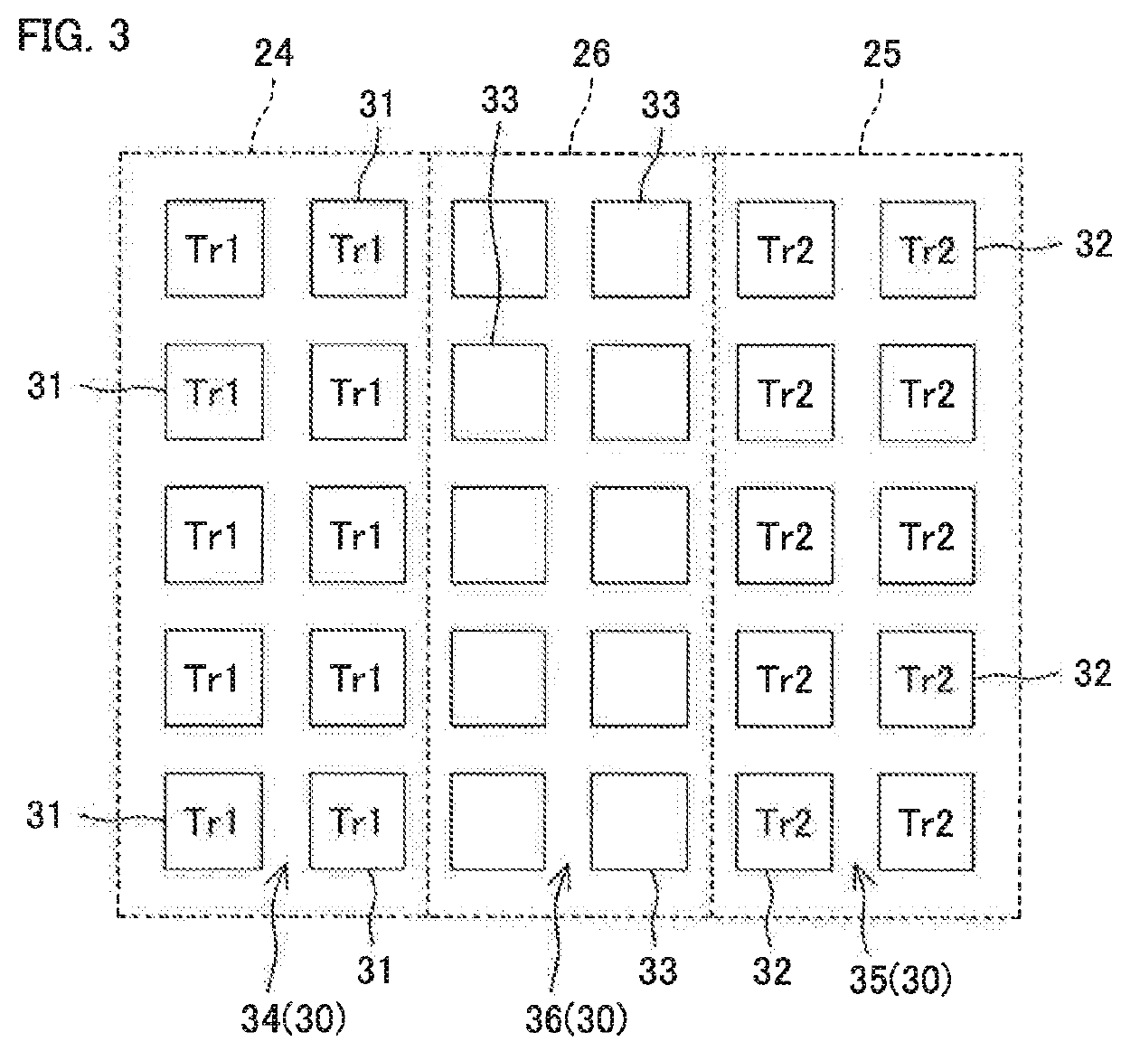
[0037]A semiconductor device includes an enhancement-mode first p-channel MISFET, an enhancement-mode second p-channel MISFET, a drain conductor electrically and commonly connected to the first p-channel MISFET and the second p-channel MISFET, a first source conductor electrically connected to a source of the first p-channel MISFET, a second source conductor electrically connected to a source of the second p-channel MISFET, and a gate conductor electrically and commonly connected to a gate of the first p-channel MISFET and a gate of the second p-channel MISFET.

[0038]In the semiconductor device, when a voltage is applied between the first source conductor S1 and the second source conductor S2 (between S1 and S2) in a state where no voltage is applied to the gate conductor G, both the MISFETs are turned on via respective parasitic diodes (internal diodes) of the first p-channel MISFET and the second p-channel MISFET. Thereby, an electric current can flow between S1 and S2. Meanwhile, ...


PUM


Abstract

A semiconductor device includes an enhancement-mode first p-channel MISFET, an enhancement-mode second p-channel MISFET, a drain conductor electrically and commonly connected to the first p-channel MISFET and the second p-channel MISFET, a first source conductor electrically connected to a source of the first p-channel MISFET, a second source conductor electrically connected to a source of the second p-channel MISFET, and a gate conductor electrically and commonly connected to a gate of the first p-channel MISFET and a gate of the second p-channel MISFET.

Description

CROSS-REFERENCE TO RELATED APPLICATIONS[0001]The present application corresponds to Japanese Patent Application No. 2016-194316 filed in the Japan Patent Office on Sep. 30, 2016, Japanese Patent Application No. 2016-194317 filed in the Japan Patent Office on Sep. 30, 2016, and Japanese Patent Application No. 2017-159596 filed in the Japan Patent Office on Aug. 22, 2017, and the entire disclosure of these applications is incorporated herein by reference.TECHNICAL FIELD[0002]The present invention relates to a semiconductor device and a semiconductor package.BACKGROUND ART[0003]Conventionally, a junction gate field effect transistor (JFET) is known as a normally-on semiconductor element.[0004]For example, Patent Document 1 (Japanese Patent Application Publication No. 2011-166673) discloses an SiC-JFET used in combination with a MOSFET.[0005]For example, Patent Document 2 (Japanese Patent Application Publication No. 2014-123665) discloses a semiconductor package including a semiconducto...

Claims


Application Information

Patent Timeline
Patent Type & Authority Applications(United States)
IPC IPC(8): H01L27/088H01L23/522H01L29/423H01L29/78H01L29/06H01L27/02
CPCH01L27/088H01L23/5226H01L29/4236H01L29/7827H01L29/0696H01L27/0255H01L23/49562H01L29/41741H01L29/4238H01L29/4933H01L29/7802H01L29/7813H01L29/7817H01L29/0619H01L29/0869H01L29/0878H01L21/823475H01L21/823487H01L27/0207H01L27/0629H01L2224/0603H01L2224/48091H01L2224/49111H01L2924/00014
Inventor NASU, KENTARONISHIDA, KENJI
Owner ROHM CO LTD
Why Eureka
Try Eureka