Photoelectric conversion device manufacturing method, photoelectric conversion device manufacturing device, and photoelectric conversion device

A technology of a photoelectric conversion device and a manufacturing method, which is applied in the fields of photovoltaic power generation, manufacturing tools, circuits, etc., can solve the problems of battery performance degradation and low effect, etc.

Inactive Publication Date: 2011-10-26
MITSUBISHI HEAVY IND LTD
View PDF2 Cites 5 Cited by
  • Summary
  • Abstract
  • Description
  • Claims
  • Application Information

AI Technical Summary

Problems solved by technology

The recrystallized region with such a low resistance has a low effect of separating the intermediate contact layer from the connection portio...

Method used


Image

  • Photoelectric conversion device manufacturing method, photoelectric conversion device manufacturing device, and photoelectric conversion device
  • Photoelectric conversion device manufacturing method, photoelectric conversion device manufacturing device, and photoelectric conversion device
  • Photoelectric conversion device manufacturing method, photoelectric conversion device manufacturing device, and photoelectric conversion device

Examples


no. 1 approach

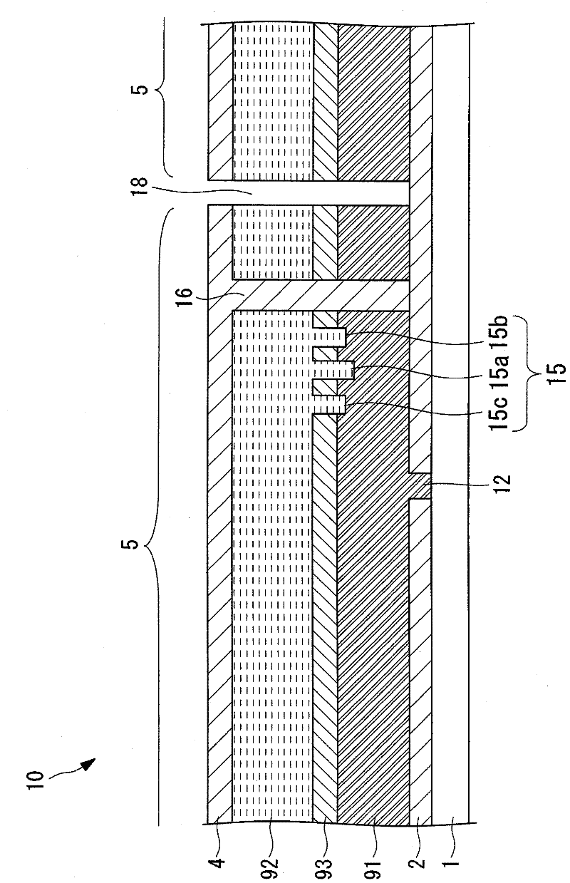
[0091] figure 1 A vertical cross-section of a tandem silicon-based thin-film solar cell (photoelectric conversion device) is shown.

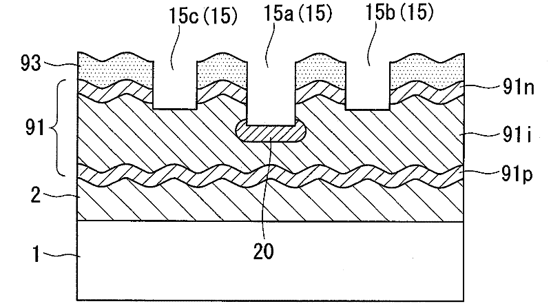
[0092] The solar cell 10 includes a glass substrate 1 as a translucent insulating substrate, a transparent electrode layer 2 , a top layer (first photoelectric conversion layer) 91 , an intermediate contact layer 93 , a bottom layer (second photoelectric conversion layer) 92 , and a back electrode layer 4 . In the present embodiment, the top layer 91 is a photoelectric conversion layer mainly comprising an amorphous silicon-based semiconductor, and the bottom layer 92 is a photoelectric conversion layer mainly comprising a crystalline silicon-based semiconductor.

[0093] Here, "silicon-based" is a generic term including silicon (Si), silicon carbide (SiC), and silicon germanium (SiGe). Furthermore, "crystalline silicon-based" means amorphous silicon-based, that is, silicon-based other than amorphous silicon-based, and includes microcrystallin...

no. 2 approach

[0138] Next, use Figure 7 and Figure 8 A second embodiment of the present invention will be described. Compared with the first embodiment, the shape of the irradiation area in this embodiment is different, and other points are the same, so only the difference will be described, and other descriptions will be omitted.

[0139] Figure 7 is the same as the first embodiment Figure 6 corresponding figure. Such as Figure 7 As shown, the irradiation area 40 is formed in a substantially rectangular shape.

[0140] As a method of forming the irradiation region 40 having a rectangular shape, a method of passing laser light through an opening formed with a rectangular hole that shields the periphery of a circular laser cross section or a method of using a kaleidoscope are mentioned.

[0141] When forming the intermediate contact layer separation groove 15, as Figure 7 As shown, one side of the irradiated area 40 is partially overlapped with one side of the adjacent irradiate...

no. 3 approach

[0145] Next, use Figure 9A to Figure 10 , the third embodiment of the present invention will be described. This embodiment differs from the first embodiment in that the depths of the processing grooves 15 are substantially uniform. Since other configurations are the same, description thereof will be omitted.

[0146] Such as Figure 9A As shown, the processing grooves 15a, 15b, and 15c shown in the first embodiment have different groove depths. In contrast, in this embodiment, if Figure 9B As shown, the groove depths of the processing grooves 15a, 15b, 15c, 15d, and 15e are substantially the same.

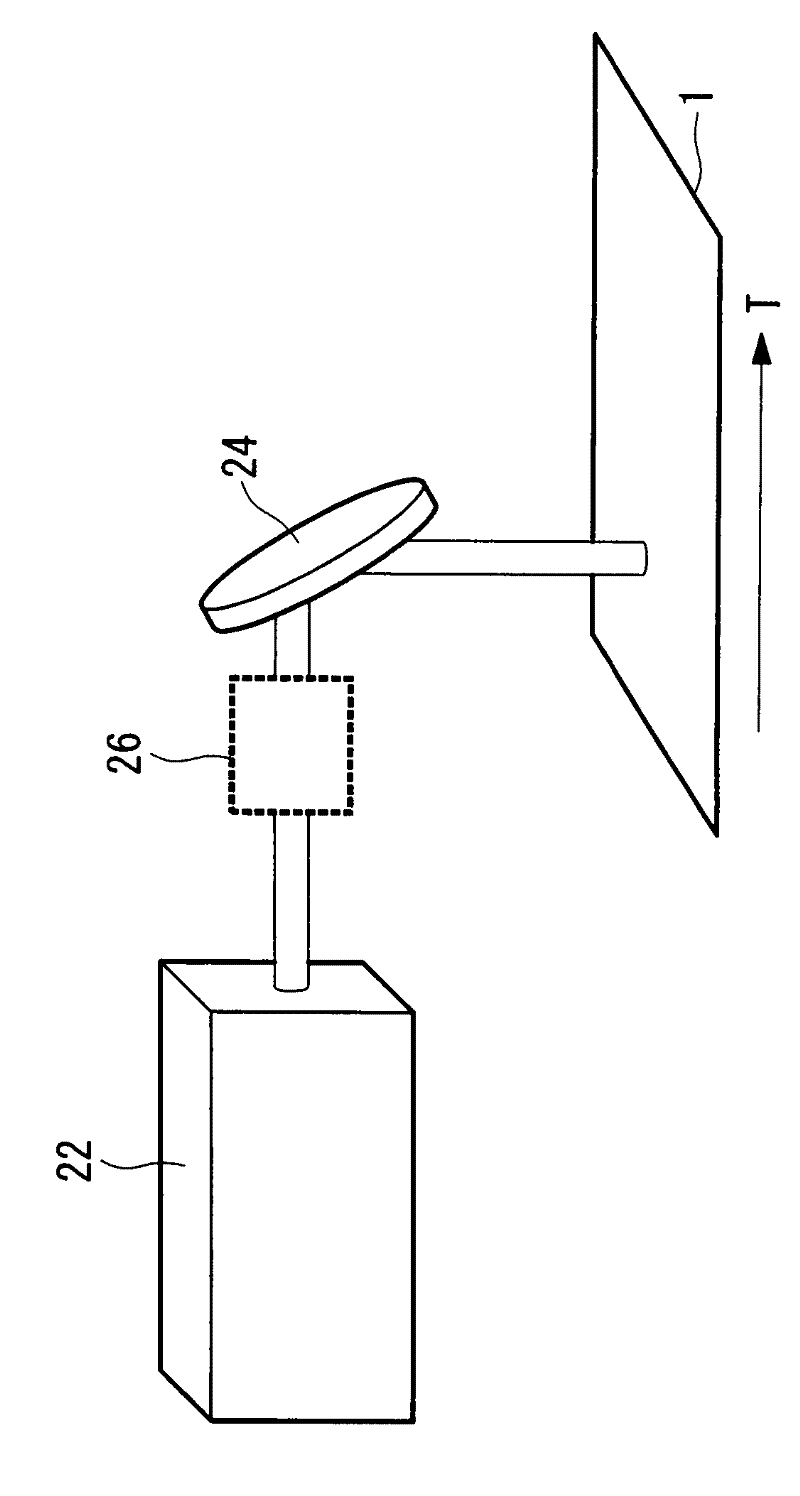
[0147] In order to make the groove depths of the processing grooves 15a, 15b, 15c, 15d, and 15e substantially uniform, it is sufficient to make the laser intensity distribution in the irradiation area uniform. Specifically, as Figure 10 As shown, the laser intensity distribution equalizing mechanism 50 is arranged in front of the total reflection mirror 24 , and the laser ...


PUM

PropertyMeasurementUnit
Areaaaaaaaaaaa
Thicknessaaaaaaaaaa
Film thicknessaaaaaaaaaa

Abstract

Provided are a photoelectric conversion device manufacturing method which can control the depth of a processing groove to a desired value, a photoelectric conversion device manufacturing apparatus and a photoelectric conversion device. The photoelectric conversion device (10) has a groove formation step which applies a pico-second laser to an intermediate contact layer separation groove (15) constituting a photoelectric conversion device (10) and forms a processing groove (15) in a predetermined scan direction by relatively moving the pico-second laser against the intermediate contact layer separation groove (15). In the groove formation step, the pico-second laser is relatively moved so that interference fringes are arranged in parallel in one direction within a radiation range corresponding to the beam diameter of the pico-second laser and the interference fringes are connected in the scan direction.

Description

technical field [0001] The present invention relates to a method for manufacturing a photoelectric conversion device, a device for manufacturing a photoelectric conversion device, and a photoelectric conversion device, and more particularly, relates to groove processing of a thin film constituting a photoelectric conversion device. Background technique [0002] Conventionally, in order to improve the photoelectric conversion efficiency of a thin-film solar cell (photoelectric conversion device), a structure in which a plurality of photoelectric conversion layers is stacked is known. For example, a tandem solar cell in which an amorphous silicon layer and a microcrystalline silicon layer are stacked is known. This tandem solar cell is formed by sequentially laminating thin films of a transparent electrode, an amorphous silicon layer, a microcrystalline silicon layer, and a rear electrode on a light-transmitting substrate. In addition, there is known a technique in which an i...

Claims


Application Information

Patent Timeline
IPC IPC(8): H01L31/04
CPCH01L31/076Y02E10/548Y02E10/52B23K26/0676B23K26/083H01L31/0463H01L31/056B23K26/0006B23K26/064B23K26/364B23K26/0624B23K26/40B23K26/359B23K2103/172B23K2103/50B23K2103/56B23K26/067H01L31/04H01L31/18
Inventor 川添浩平宇田和孝马场智义石出孝中尾祯子
Owner MITSUBISHI HEAVY IND LTD
Why Eureka
Try Eureka