
FPGA-based Interface Signal Remapping Method

a signal remapping and interface technology, applied in the field of nuclear power system technology, can solve the problems of poor readability of signal name in the fpga chip, data signal transmission rate error, poor readability and debugging, etc., and achieve the effects of improving reliability, readability and debugging, and poor readability of signal nam

Active Publication Date: 2018-04-19
STATE NUCLEAR POWER AUTOMATION SYST ENGCO
View PDF0 Cites 7 Cited by
  • Summary
  • Abstract
  • Description
  • Claims
  • Application Information

AI Technical Summary

Benefits of technology

The invention provides an FPGA-based interface signal remapping method that can reliably transmit external signals into an FPGA chip. This method uses an I / O module to process signal excursions, signal collision, metastable state, and data transmission errors, while a Core module focuses on execution of communication, arithmetical operation, logical processing, and other functions with improved reliability, readability, and debuggability. The invention also introduces a master clock signal outside the FPGA chip through a global clock pin of the FPGA chip to prevent and alleviate problems such as master clock signal excursion, data signal collision, metastable register output, transmission rate error, and poor readability of signal name. Overall, the invention improves the efficiency and reliability of the FPGA chip in transmitting and processing external signals.

Problems solved by technology

Some problems may occur in the process, including the master clock signal excursion, data collision due to two-way data signal input / output through a single signal line, metastable register output due to asynchronous reset signal, transmission rate error of data signals between asynchronous clock domains, and poor readability of signal name in the FPGA chip.
However, for design of FPGA in the nuclear power instrumentation and control system in the prior art, the master clock signal transmission, two-way data transmission and signal transmission, data transmission between asynchronous clock domains, asynchronous reset signal transmission and mapping of different signal names are located in different functional modules and have poor readability and debuggability, which are not conducive to the modular design and debugging of FPGA.
Moreover, there is no technology available for nuclear power protection system platform that is capable of reliably transmitting all external signals into the FPGA chip in the protection system platform.

Method used


Image

  • FPGA-based Interface Signal Remapping Method
  • FPGA-based Interface Signal Remapping Method
  • FPGA-based Interface Signal Remapping Method

Examples


Embodiment Construction

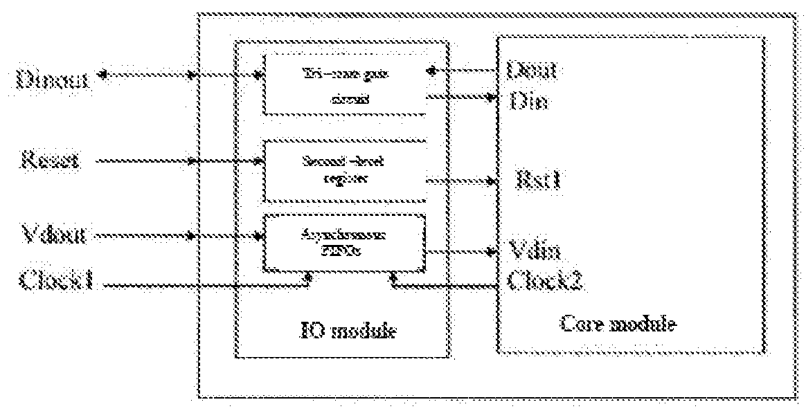
[0019]The embodiment of the invention is described in detail in combination with description of accompanying drawings. However, the embodiment is not used to limit the invention. Any structures and changes similar to the invention should be incorporated in the protection scope of the invention. All caesura signs in the invention refer to “and”.

[0020]FIG. 1 shows an FPGA-based interface signal remapping method of the embodiment of the invention, characterized by:

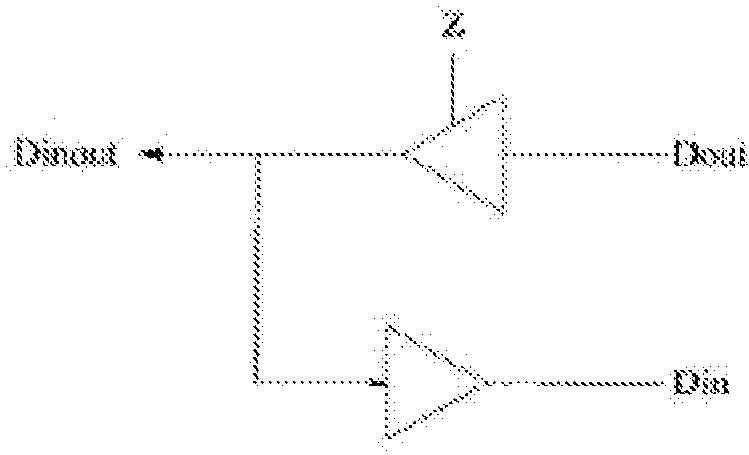
[0021]dividing an internal programmable logic of an FPGA chip into two independent modules, with one module being an I / O module and the other module being a Core module, using the I / O module to process the signal excursion occurring when an external signal is input to or output from the FPGA chip, signal collision caused by line multiplexing, metastable state in a data transmission process, and a data transmission error between asynchronous clock domains; using the Core module to implement logical processing and computing; an...


PUM


Abstract

An FPGA-based interface signal remapping method, relates to the technical field of nuclear power system, and solves the technical problems of poor reliability, readability and debuggability in the prior art. The method comprises dividing an internal programmable logic of an FPGA chip into two independent modules, with one module being an I / O module and the other module being a Core module, using the I / O module to process signal excursion occurring when an external signal is input to or output from the FPGA chip, signal collision caused by line multiplexing, metastable state in a data transmission process, and a data transmission error between asynchronous clock domains, using the Core module to implement logical processing and computing; and introducing a master clock signal outside the FPGA chip into the FPGA chip through a global clock pin of the FPGA chip. The method provided in the invention is suitable for a nuclear power protection system platform.

Description

FIELD OF THE INVENTION[0001]The present invention relates to a nuclear power system technology, in particular to a technology of FPGA-based interface signal remapping method.DESCRIPTION OF THE RELATED ART[0002]FPGA technology has the advantages of regular structure and high reliability, and the FPGA technology is increasingly used in the field of instrumentation and control system to achieve a variety of functions, including communication protocols as well as logical processing and control. When using an FPGA chip, it is necessary to input the external signal into the chip for processing. Some problems may occur in the process, including the master clock signal excursion, data collision due to two-way data signal input / output through a single signal line, metastable register output due to asynchronous reset signal, transmission rate error of data signals between asynchronous clock domains, and poor readability of signal name in the FPGA chip.[0003]For transmission of two-way data si...

Claims


Application Information

Patent Timeline
IPC IPC(8): G06F13/42G06F1/24G06F1/12G06F5/14
CPCG06F13/4239G06F1/24G06F1/12G06F5/14G06F2205/126G06F13/40
Inventor ZHANG, JIANJIANG, QUNXINGWANG, XIAOKAI
Owner STATE NUCLEAR POWER AUTOMATION SYST ENGCO
Learn More