
Semiconductor memory device with improved program verification reliability

a semiconductor memory and program verification technology, applied in the field of semiconductor memory devices, can solve problems such as loss of stored data, and achieve the effect of improving the threshold voltage distribution of selection transistors in the program operation of semiconductor memory devices

Active Publication Date: 2018-05-10
SK HYNIX INC
View PDF2 Cites 3 Cited by
  • Summary
  • Abstract
  • Description
  • Claims
  • Application Information

AI Technical Summary

Benefits of technology

The patent aims to improve the performance of a semiconductor memory device by improving the threshold voltage distribution of the selection transistor during program operation. The technical effect of this patent is to enhance the efficiency and reliability of the semiconductor memory device's program operation.

Problems solved by technology

In the volatile memory device, a power turn-off may cause loss of stored data therein.

Method used


Image

  • Semiconductor memory device with improved program verification reliability
  • Semiconductor memory device with improved program verification reliability
  • Semiconductor memory device with improved program verification reliability

Examples


Embodiment Construction

[0026]Examples of various embodiments are illustrated in the accompanying drawings and described further below. It will be understood that the discussion herein is not intended to limit the claims to the specific embodiments described. On the contrary, it is intended to cover alternatives, modifications, and equivalents as may be included within the spirit and scope of the present disclosure as defined by the appended claims.

[0027]Example embodiments will be described in more detail with reference to the accompanying drawings. The present disclosure, however, may be embodied in various different forms, and should not be construed as being limited to only the illustrated embodiments herein. Rather, these embodiments are provided as examples so that this disclosure will be thorough and complete, and will fully convey the aspects and features of the present disclosure to those skilled in the art.

[0028]It will be understood that, although the terms “first”, “second”, “third”, and so on ...


PUM


Abstract

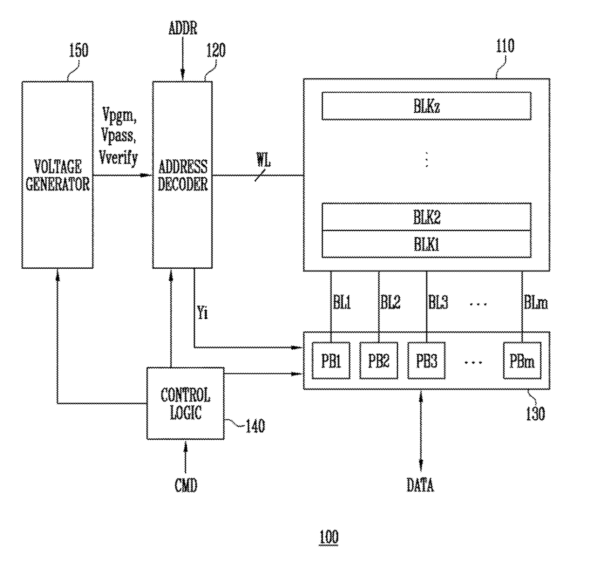
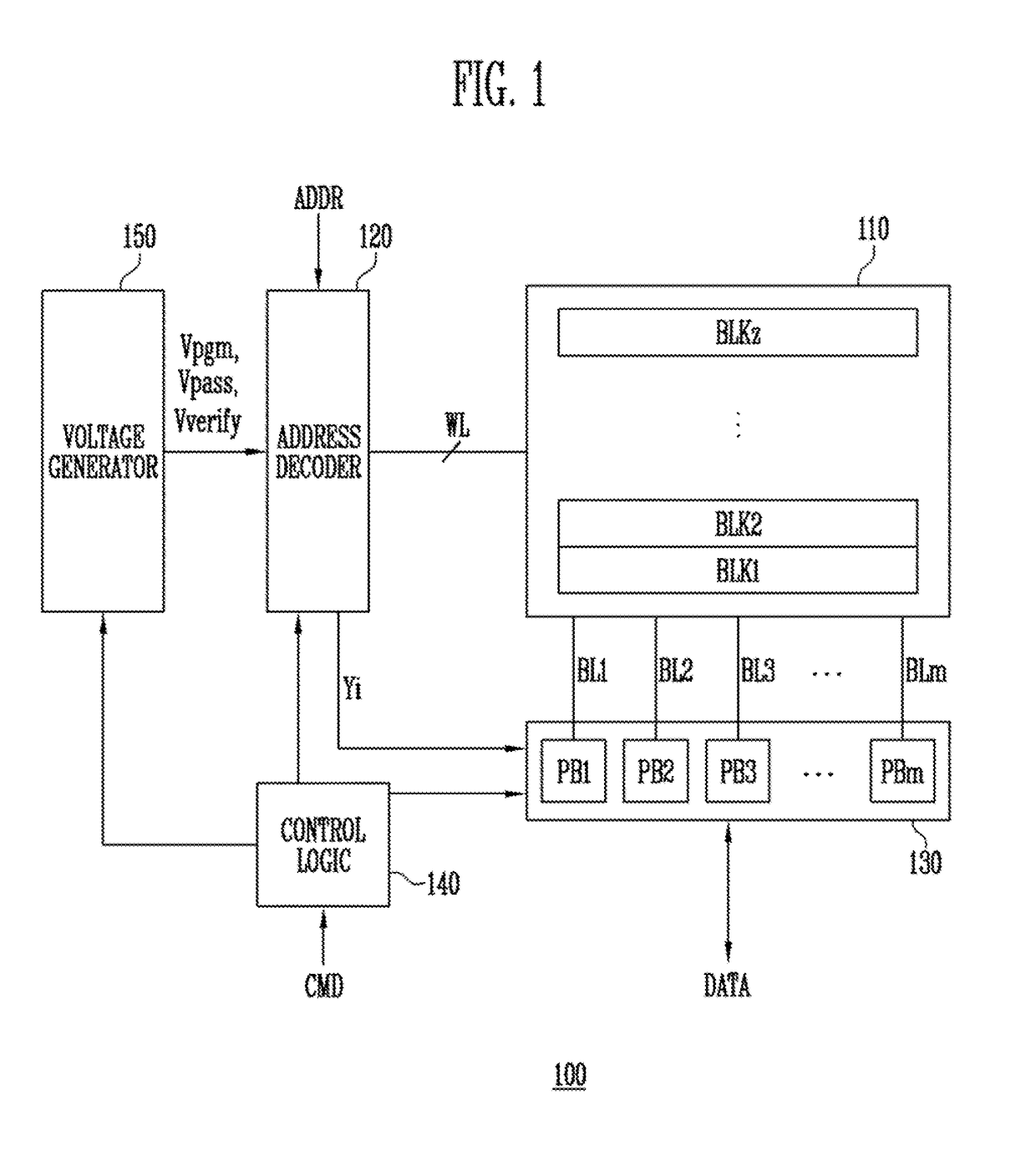
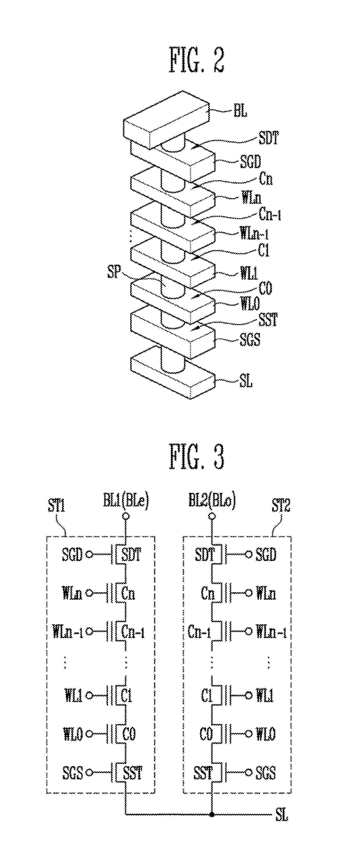
A semiconductor memory device includes a memory cell array including first and second groups of memory strings respectively coupled to first and second groups of bit-lines, wherein the first and second groups of memory strings respectively include first and second groups of selection transistor cells; a peripheral circuit suitable for applying a program voltage, and performing program verification operation for the memory cell array; and a control logic suitable for controlling the peripheral circuit to perform a first program verification operation for the first group of selection transistor cells and a second program verification operation for the second group of selection transistor cells.

Description

CROSS-REFERENCE TO RELATED APPLICATION[0001]This application is a division of U.S. patent application Ser. No. 14 / 997,731 filed on Jan. 18, 2016, which claims priority to Korean patent application number 10-2015-0102494, filed on Jul. 20, 2015. The disclosure of each of the foregoing applications is herein incorporated by reference in its entirety.BACKGROUND1. Field[0002]The present disclosure relates to an electronic device, and more particularly, to a semiconductor memory device and an operation method thereof.2. Discussion of Related Art[0003]A semiconductor memory device may be implemented using a semiconductor such as silicon (Si), germanium (Ge), gallium arsenide (GaAs), indium phosphite (InP) or the like. The semiconductor memory device may be classified into volatile and nonvolatile memory devices.[0004]In the volatile memory device, a power turn-off may cause loss of stored data therein. The volatile memory device may include Static RAM (SRAM), Dynamic RAM (DRAM), Synchrono...

Claims


Application Information

Patent Timeline
Patent Type & Authority Applications(United States)
IPC IPC(8): G11C16/34G11C16/24G11C16/04G11C16/10
CPCG11C2216/16G11C16/24G11C16/3459G11C16/0483G11C16/10
Inventor PARK, EUN YOUNG
Owner SK HYNIX INC
Learn More