Method of finfet contact formation

a contact formation and finfet technology, applied in the field of semiconductor devices, can solve problems affecting the quality of semiconductor devices, and achieve the effects of reducing gate capacitance, avoiding leakage between the gate and the contact, and reducing the risk of leakag

Active Publication Date: 2018-05-24
SEMICONDUCTOR MANUFACTURING INTERNATIONAL (BEIJING) CORP +1
View PDF15 Cites 2 Cited by
  • Summary
  • Abstract
  • Description
  • Claims
  • Application Information

AI Technical Summary

Benefits of technology

[0005]Embodiments of the present invention relate to the field of semiconductor technology. More particularly, the embodiments relate to a semiconductor device and a method for manufacturing the device. In an embodiment, a non-self-aligned process is used to generate the upper half portion of a contact hole. A sidewall dielectric layer is formed on the sidewalls of the upper half portion of the contact hole. The lower half of the contact hole is etched using the sidewall dielectric as a self-aligned mask. Leakage between the gate and the contact can be avoided or reduced, and the gate capacitance can be reduced.

Problems solved by technology

A short between a gate electrode and a contact to an active region can lead to leakage and adversely affect the quality of the semiconductor device.

Method used


Image

  • Method of finfet contact formation
  • Method of finfet contact formation
  • Method of finfet contact formation

Examples


Embodiment Construction

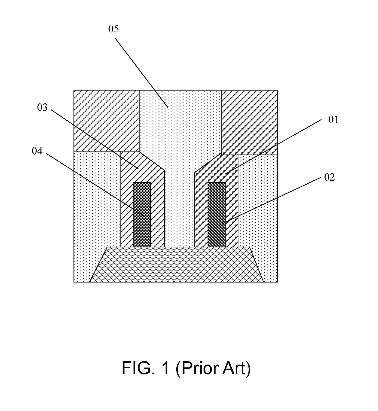
[0047]Embodiments of the present invention relate to the field of semiconductor technology. More particularly, the embodiments relate to a semiconductor device and a method for manufacturing the device. In an embodiment, a non-self-aligned process to generate the upper half portion of a contact hole. A sidewall dielectric layer is formed on the sidewalls of the upper half portion of the contact hole. The lower half of the contact hole is etched using the sidewall dielectric as a self-aligned mask. Leakage between the gate and the contact can be avoided or reduced, and the gate capacitance can be reduced.

[0048]Various exemplary embodiments of the present invention will now be described in detail with reference to the accompanying drawings. It should be noted that the relative arrangement, numerical expression, and numerical values of the components and steps set forth in these embodiments, unless otherwise specified, do not limit the scope of the invention. At the same time, it will ...


PUM


Abstract

A method of manufacturing a semiconductor device includes providing a substrate structure, which includes a substrate, one or more semiconductor fins on the substrate, a gate structure on each fin, an active region located in said fins, and an interlayer dielectric layer covering at the active region. The method includes forming a hard mask layer over the interlayer dielectric layer and the gate structure, and using an etch process with a patterned etch mask, forming a first contact hole extending through the hard mask layer and extending into a portion of the interlayer dielectric layer, using patterned a mask. The method further includes forming a sidewall dielectric layer on sidewalls of the first contact hole, and using an etch process with the sidewall dielectric layer as an etch mask, etching the interlayer dielectric layer at bottom of the first contact hole to form a second contact hole extending to the active region.

Description

CROSS-REFERENCES TO RELATED APPLICATIONS[0001]This application claims priority to Chinese patent application No. 201611061525.1, filed on Nov. 23, 2016, the content of which is incorporated herein by reference in its entirety.BACKGROUND OF THE INVENTION[0002]The present invention relates to the field of semiconductor technology, and more particularly to a semiconductor device and a method for manufacturing the device.[0003]FinFET (Fin Field-Effect Transistor) is a new complementary metal oxide semiconductor (CMOS) transistor structure, which has many advantages, such as good control of short channel effects, high drive current, low power consumption, and small size, etc. FinFET can offer hope that the Moore's Law device scaling can be extended. Recently, FinFET has begun to be used in the 14-nm node of technology. Currently, in FinFET, the process of forming contacts to active regions often uses a self-aligned process to form the contact hole, and then a conductive material is depos...

Claims


Application Information

Patent Timeline
Patent Type & Authority Applications(United States)
IPC IPC(8): H01L21/8238H01L21/84H01L29/417H01L29/423H01L29/78H01L29/66H01L29/06
CPCH01L21/823821H01L21/845H01L29/41791H01L29/4238H01L29/785H01L29/66583H01L29/0607H01L2029/7858H01L29/401H01L29/66795H01L21/76897H01L21/76831
Inventor HAN, QIUHUATANG, LONGJUAN
Owner SEMICONDUCTOR MANUFACTURING INTERNATIONAL (BEIJING) CORP
Why Eureka
Try Eureka