Permutated Ring Network

a ring network and network technology, applied in data switching networks, loop networks, multiplex communication, etc., can solve the problems of increasing the number of intra-chip communication nodes, the demand for on-chip data bandwidth, and the scaling of problems, so as to achieve the effect of reducing the challenge of clock distribution

Active Publication Date: 2018-05-24
DEGIRUM CORP
View PDF6 Cites 9 Cited by
  • Summary
  • Abstract
  • Description
  • Claims
  • Application Information

AI Technical Summary

Benefits of technology

[0014]Accordingly, the present invention provides a permutated ring network that includes a plurality of communication nodes and a plurality of bi-directional source-synchronous ring networks, each having a plurality of data transport stations. Each of the communication nodes is coupled to one of the data transport stations in each of the plurality of bi-directional source-synchronous ring networks. A source synchronous technique used to transmit data on the ring networks mitigates the clock distribution challenges. The number of bi-directional source-synchronous ring networks can be selected to provide the bandwidth required by communications between the various communication nodes. In this manner, the permutated ring network of the present invention can be readily scaled.

Problems solved by technology

On-chip communication systems exhibit scaling problems, and the number of intra-chip communication nodes and the demand for on chip data bandwidth are ever increasing.
Physical limitations for on-chip communications include the length of on-chip wires, which is critical to the delay and operating frequency.
Long wires severely degrade performance, as the frequency has a first order effect on the network bandwidth.
High fan-out nodes further degrade the bandwidth by creating place and route congestion, and adding more gate and wire delays to the network.
Clock distribution imposes a great obstacle in building large scale high bandwidth on-chip networks.
More specifically, clock skew will limit the operating frequency of the network, and the required clock power may impose limits on the network.
In addition, challenges exist in typical communication network topologies, with regard to scaling up the number of communication nodes and maintaining high operating frequencies.
For each of these network topologies, the delay and operating frequency of the system will degrade severely as the wire length of the interconnects increase.
Moreover, high fan-out nodes will cause place and route congestions that will further degrade the speed and power performance of the system.
However, the fan-out of the nodes undesirably increases as the number of nodes (N) increase, with a scaling factor of Log(N).
Because these network topologies are implemented using on-chip interconnects that are not perfect wires, the delay and operating frequency of these networks will degrade severely as wire lengths increase.
In addition, high fan-out nodes will cause place and route congestions that will degrade the speed and power performance of the networks.
However, increasing the number of on-chip nodes will degrade the system bandwidth due to increases in wire length and routing congestion when conventional network topologies are used.
Consequently, an on-chip bandwidth scaling ‘wall’ effectively limits the growth of on-chip communication networks.

Method used


Image

  • Permutated Ring Network
  • Permutated Ring Network
  • Permutated Ring Network

Examples


Embodiment Construction

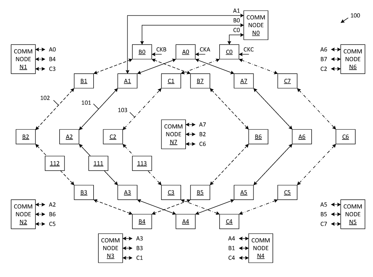
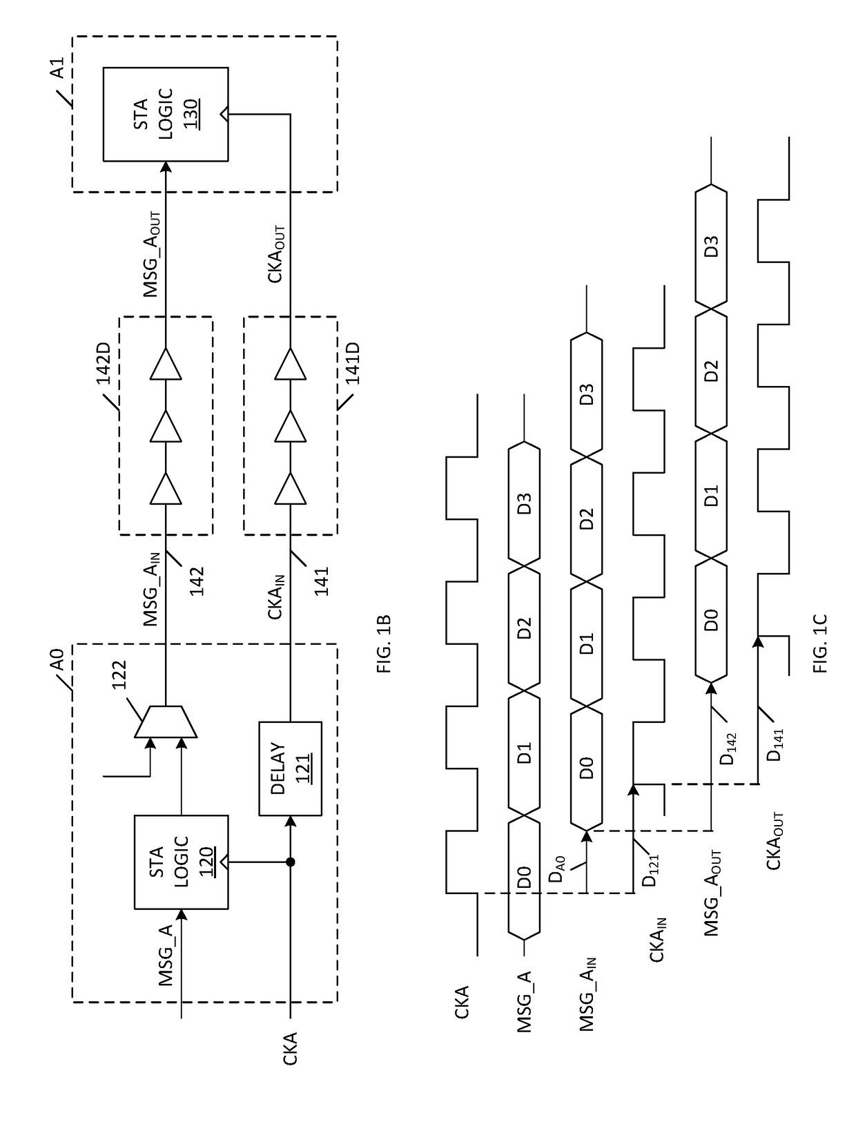
[0031]In general, the present invention provides a permutated ring network architecture that includes a plurality of bi-directional source-synchronous communication rings that are shared among a plurality of network nodes. A source synchronous technique is used to mitigate the clock distribution challenges, wherein a transmitting node sends both a clock and data to a receiving node. The receiving node latches the data using the received clock. The clock fan-out is limited to the size of the data bus width. The clock skew is set by the delay relationship between the clock and the corresponding data. Note that the source synchronous technique will only work with a point-to-point interconnect (e.g., a ring network). Numerous on-chip interconnect resources are required to implement a point-to-point network. However, Moore's law predicts that the number of metal layers will scale upward, the metal pitch will decrease, and more wires will be available per unit area as process technologies...


PUM


Abstract

A permutated ring network includes a plurality of bi-directional source-synchronous ring networks, each having a plurality of data transport stations, and a plurality of communication nodes. Each of the communication nodes is coupled to one of the data transport stations in each of the plurality of bi-directional source-synchronous ring networks.

Description

RELATED APPLICATIONS[0001]This application claims priority from U.S. Provisional Patent Application 62 / 425,798, entitled “Permutated Ring Network”, which was filed on Nov. 23, 2016, and is incorporated by reference herein.FIELD OF THE INVENTION[0002]The present invention relates to a permutated ring network having a plurality of rings, which provides a scalable, high-bandwidth, low-latency point-to-point on-chip communications solution.RELATED ART[0003]On-chip communication systems exhibit scaling problems, and the number of intra-chip communication nodes and the demand for on chip data bandwidth are ever increasing. High speed serializing / deserializing (SERDES) communication protocols are trending toward providing an operating bandwidth of 100 Gb / sec per pin. Thus, a chip having 1000 pins may require a chip input / output (I / O) bandwidth of up to 100 Terabit / sec. There is a need to provide on-chip communication bandwidth to support these specifications. Examples of systems requiring ...

Claims


Application Information

Patent Timeline
Patent Type & Authority Applications(United States)
IPC IPC(8): H04L12/42H04J3/08H04J3/06H04L12/741H04L45/74
CPCH04L12/422H04J3/085H04J3/0658H04L45/745H04L2012/421H04L12/4637
Inventor TAM, KIT S.LEE, WINSTON
Owner DEGIRUM CORP
Why Eureka
Try Eureka