Process for producing an electromechanical device

a technology of electromechanical devices and process, which is applied in the direction of microstructural devices, microstructure devices, microstructure technology, etc., can solve the problems of limiting the choice of usable materials, affecting the use of materials, and affecting the performance of the device, so as to promote molecular adhesion, increase bonding energy, and avoid stiction.

Active Publication Date: 2018-05-31
COMMISSARIAT A LENERGIE ATOMIQUE ET AUX ENERGIES ALTERNATIVES
View PDF2 Cites 5 Cited by
  • Summary
  • Abstract
  • Description
  • Claims
  • Application Information

AI Technical Summary

Benefits of technology

[0056]An important element is that the dimensions of the central portion 1c and of the first apertures 4 be determined such that the central portion 1c is sufficiently rigid to prevent any stiction effect between the central portion 1c and, on the one hand, the adjacent portion 1a (lateral stiction) or, on the other hand, the lower layer 3 (vertical stiction). This is a notable advantage of the invention: the sacrificial layer is removed while the central portion 1c is rigid enough to prevent the occurrence of a stiction effect. In addition, depending on the topology of the first apertures 4, anchors 1b may reinforce the rigidity of the central portion 1c. Specifically, during this removal, the central portion has an elasto-capillary number higher than 1, this making it possible to avoid the occurrence of a stiction. The elasto-capillary number is defined below. Specifically, regarding physical parameters that may possibly promote its appearance, stiction depends on the elastic stiffness of the microstructure 1c, and on the thickness of the intermediate layer 2. In this step, it is ensured that these parameters are dimensioned so as to prevent stiction, this amounting to an elastic-capillary number higher than 1. Conversely to the prior art, the removal of the sacrificial layer is not a final step, in which the movable portion of the electromechanical device is released, but an intermediate step of the process, implemented without risk of stiction. The process is thus more reliable than processes of the prior art based on release of a movable microstructure by wet etching.
[0057]FIGS. 3G and 3H show a step of joining what is called a blocking layer to the upper layer 1. In FIG. 3G, a substrate 20, called the auxiliary substrate, a first end of which is formed by a lower layer 21, called the blocking layer, has been illustrated. This auxiliary substrate includes a sacrificial layer 22, borne by a carrier layer 23. The auxiliary layer 20 may be an SOI substrate, in which case the lower layer 21 is a layer of single-crystal silicon, the sacrificial layer 22 consists of SiO2 and the carrier layer 23 is formed from single-crystal silicon.
[0058]As shown in FIG. 3H, the auxiliary substrate 20 is applied to the base substrate 10, such that the lower layer 21 of the auxiliary substrate presses against the upper layer 1 of the base substrate 10 and, as a result, bonds to the latter. According to a first possibility, the upper layer 1 of the base substrate 10 and the lower layer 21 of the auxiliary substrate 20 are bonded to each other by molecular bonding. A chemical clean and a preparation phase may be carried out before these two layers are brought into contact, a vacuum anneal being carried out thereafter. The preparation phase, known to those skilled in the art, consists in activating the surfaces of each layer with a view to promoting molecular adhesion between the two layers once they are brought into contact. It will be noted that, because of the mechanical rigidity of the central portion 1c, there is no risk of stiction during the cleaning and preparation phases preceding the bonding. An example of preparation consists in making the surfaces hydrophobic with a 15- to 20-second treatment in HF diluted to 1%. The annealing phase allows the bonding energy to be increased. It may for example be carried out at a temperature exceeding 600° C., or even 1200° C., for 2 hours.
[0059]According to one variant, before the two substrates are brought into contact, the lower layer 21 of the auxiliary substrate 20 is covered with an SiO2 oxide layer advantageously formed by thermal oxide growth. When brought into contact, the upper layer 1 of the base substrate 10 and the lower layer 21 of the auxiliary substrate 20 then bond by hydrophilic molecular bonding. Alternatively, or in addition, an oxide layer may be formed on the upper layer 1 of the base substrate 10, this also allowing the lower layer 21 of the auxiliary substrate 20 to be bonded to the upper layer 1 of the base substrate 10 by hydrophilic molecular bonding.
[0060]The following step, illustrated in FIG. 3I, consists in removing the carrier layer 23 of the auxiliary substrate, and the sacrificial layer 22 of the latter. The carrier layer 23 may be removed by mechanical abrasion, or by chemical etching. The sacrificial layer 22 then acts as stop layer for the etching. The latter may then be removed by chemical etching, in such a way as to maintain the integrity of the lower layer 21. When the lower layer is made of single-crystal silicon and the sacrificial layer 22 is formed from SiO2, an HF chemical etch may for example be used. The lower layer 21 then forms a layer, called a blocking layer 6, on the base substrate 10.
[0061]According to one variant, the auxiliary substrate may be formed from a carrier layer 23, for example made of single-crystal silicon, covered with a lower layer 21 of silicon oxide SiO2. The latter may be joined to the upper layer 1 of the base substrate 10 by hydrophilic molecular bonding. The carrier layer 23 is then removed by mechanical abrasion followed by a chemical etch with tetramethylammonium hydroxide (TMAH). The blocking layer 6 is then the residual layer of silicon oxide, i.e. the lower layer remaining after the carrier layer 23 has been removed.

Problems solved by technology

The first drawback is that there is a risk that the microstructure 105 of the device will be damaged during the releasing step.
Specifically, although the etch rate of certain materials other than the material of the sacrificial layer 102 is low, it is not however zero and structures made from these materials may be damaged and made non-functional.
As a result, recourse to a chemical etch restricts the choice of usable materials.
However, such an alternative then requires the protective material to be removed, this possibly also affecting certain materials.
Making provision to carry out a wet etch from the back side decreases the risk of vertical stiction (i.e. of adhesion of the microstructure 205 to the lower layer 203) but increases the complexity of the process.
This requires an etch the uniformity of which is high to be used, this possibly proving to be difficult when various cavities, of various sizes, are to be etched in the same substrate, the etch then being faster in larger cavities than in smaller cavities.

Method used


Image

  • Process for producing an electromechanical device
  • Process for producing an electromechanical device
  • Process for producing an electromechanical device

Examples


first embodiment

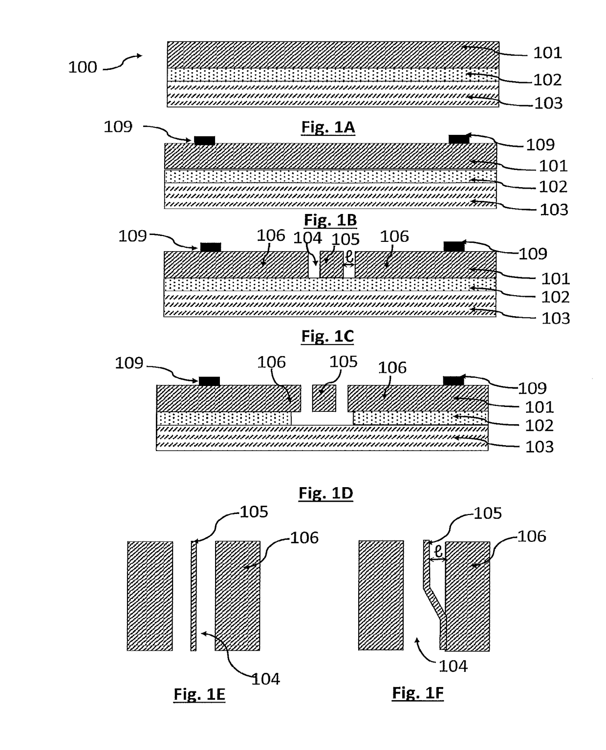
[0046]FIGS. 3A to 3M illustrate the steps of a first embodiment intended to produce a microelectromechanical system (MEMS) or nanoelectromechanical system (NEMS).

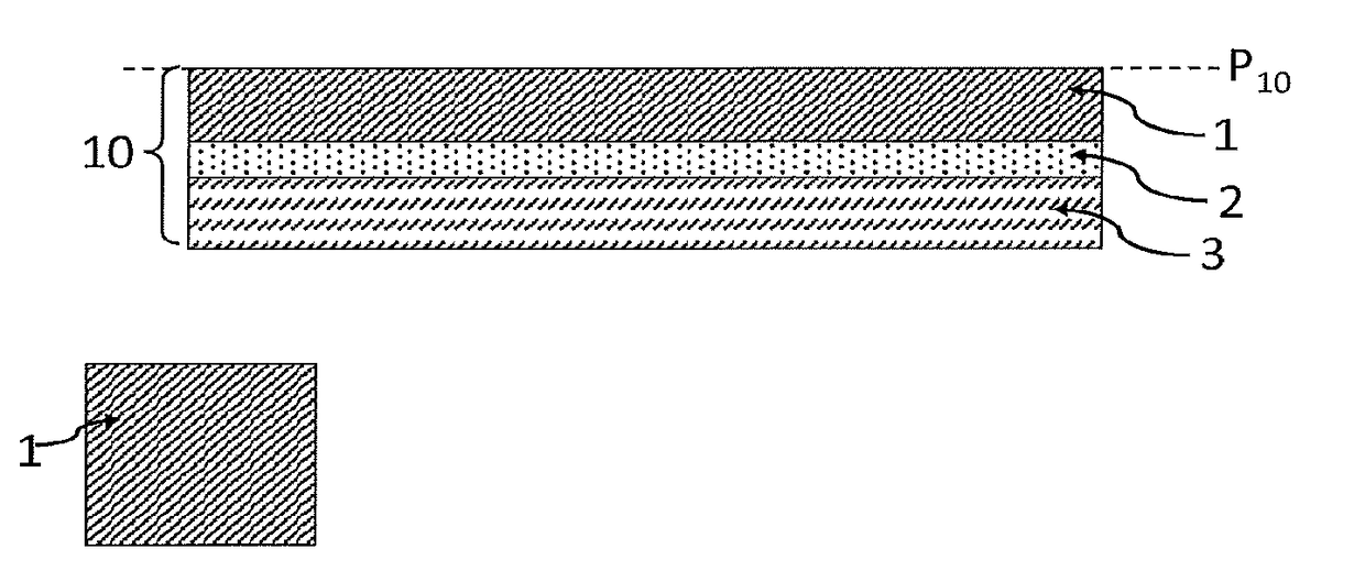
[0047]A silicon-on-insulator (SOI) substrate 10, called the base substrate, is provided. This substrate comprises an insulating intermediate layer 2 placed between an upper layer 1 made of silicon, and preferably made of single-crystal silicon, and a lower layer 3 made of silicon. These three layers lie parallel to a plane P10 called the plane of the substrate. The intermediate layer 2 consists of what is called a buried oxide layer, usually designated by the acronym BOX (for Buried OXide). It is preferably silicon oxide (SiO2). The intermediate layer 2 serves as an etch stop layer and as a sacrificial layer, as described below. A dielectric is preferably used to form this layer, because this makes it possible to avoid short-circuiting a plurality of electromechanical devices formed in the same substrate. The thickness of t...

third embodiment

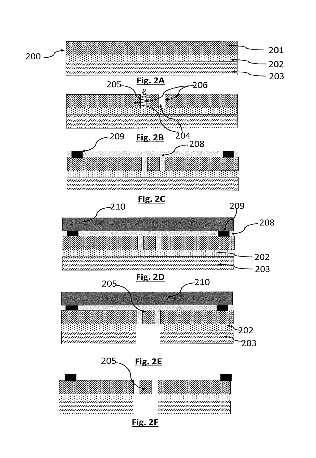
[0081]FIGS. 6A to 6D show various steps for producing a substrate according to this FIG. 6A shows the formation of first apertures 4 and the formation of a cavity 5 by removal of a portion of the sacrificial layer 2 located between said first apertures. FIG. 6B shows what are called post-processing steps, which are carried out after the blocking layer 6 has been applied to the upper layer 1, these post-processing steps resulting in the formation of functional elements 9 on the surface of this blocking layer 6. By way of nonlimiting example, the formation of a metal layer 9.1, of dielectric layers 9.2 and of hydrophobic layers 9.3 has been shown. FIG. 6C shows the substrate after a beam-shaped movable portion 7.1 of the device has been defined, the etched trench 8 encircling this movable portion. FIG. 6D shows another example embodiment, in which the etched trench 8 defines not one movable portion 7.1 but three beam-shaped movable portions. It will be understood that, depending on t...


PUM

PropertyMeasurementUnit
thicknessaaaaaaaaaa
widthaaaaaaaaaa
thicknessaaaaaaaaaa

Abstract

The invention is a process for producing an electromechanical device including a movable portion that is able to deform with respect to a fixed portion. The process implements steps based on fabrication microtechnologies, applied to a substrate including an upper layer, an intermediate layer and a lower layer. These steps are:a) forming first apertures in the upper layer;b) forming an empty cavity in the intermediate layer, which step is referred to as a pre-release step because a central portion of the upper layer lying between the first apertures is pre-released;c) applying what is called a blocking layer to the upper layer, this layer covering the first apertures, the blocking layer and the central portion together forming a suspended microstructure above the empty cavity;d) producing a boundary trench in the suspended microstructure, so as to form, in this microstructure, a movable portion and a fixed portion, the movable portion forming a movable member of the electromechanical device.

Description

TECHNICAL FIELD[0001]The technical field of the invention is the fabrication of MEMS- or N EMS-type electromechanical devices, intended to form resonators, switches, or movement detectors.PRIOR ART[0002]Microelectromechanical systems (MEMS) or nanoelectromechanical systems (NEMS) are commonly used in many industrial fields, where they are used as actuators or as detectors. To give just a few examples, such devices are found in accelerometers, movement or pressure sensors, mobile telephones and this list is far from being exhaustive. Application of these devices to biological or medical analysis has also been the subject of much work.[0003]Many electromechanical devices include a thin movable structure that is said to be suspended above a substrate, the suspended structure being able to deform under the effect of a stress, whether it be a stress due to pressure, or the application of an electric field, via a capacitive effect, or the effect of gravity or even the application of an ac...

Claims


Application Information

Patent Timeline
Patent Type & Authority Applications(United States)
IPC IPC(8): B81C1/00
CPCB81B2201/0214B81C2201/0176B81C1/00476B81C1/00944B81C2201/0109B81B2203/0118B81C2201/019B81B2201/0264B81C2201/0181B81C2201/0178B81B3/0021B81C2201/0132B81C1/00952B81C2201/053
Inventor AGACHE, VINCENTBALERAS, FRANCOIS
Owner COMMISSARIAT A LENERGIE ATOMIQUE ET AUX ENERGIES ALTERNATIVES
Why Eureka
Try Eureka