Photovoltaic device

a photovoltaic and solar energy technology, applied in the field of photovoltaic devices, can solve the problems of high material cost, high cost of manufacturing devices that capture solar energy, and historically impede its widespread use, and achieve the effect of improving stability and improving stability

Active Publication Date: 2018-06-14
OXFORD PHOTOVOLTAICS
View PDF1 Cites 14 Cited by
  • Summary
  • Abstract
  • Description
  • Claims
  • Application Information

AI Technical Summary

Benefits of technology

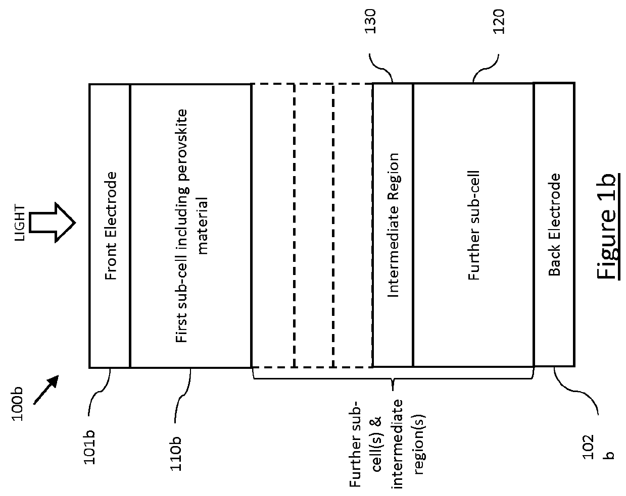
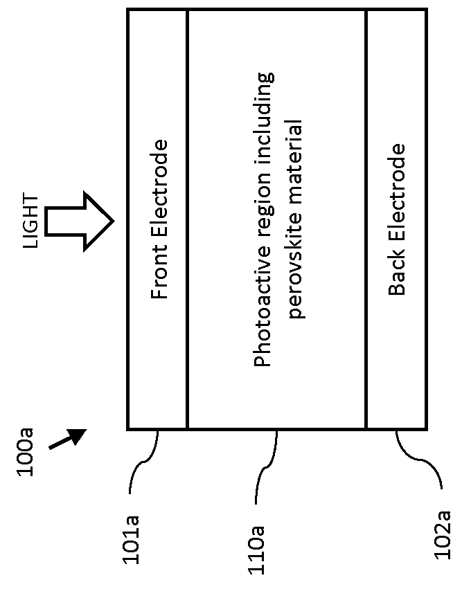
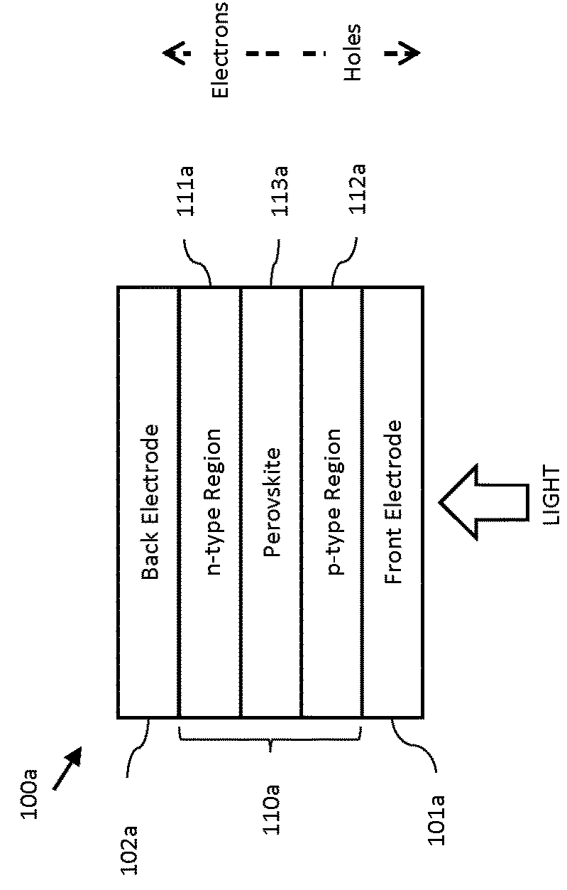
[0012]The inventors have developed a photoactive perovskite material that has both a bang gap that makes it suitable for use in multi-junction photovoltaic devices and improved stability. In particular, the inventors have developed a photoactive perovskite material that has a band gap in the region of 1.6 to 2.3 eV, for use in a top sub-cell in a tandem photovoltaic device in combination with a lower band gap bottom sub-cell, and that has improved stability. The inventors have also developed methods and formulations for producing such a photovoltaic device.

Problems solved by technology

To this end, solar energy is seen as one of the most promising technologies, nevertheless, the high cost of manufacturing devices that capture solar energy, including high material costs, has historically hindered its widespread use.
If the band gap is too high, most daylight photons cannot be absorbed; if it is too low, then most photons have much more energy than necessary to excite electrons across the band gap, and the rest will be wasted.
In comparison, equivalent single-anion perovskites are relatively unstable, with bleaching occurring quickly when fabricating films from the single halide perovskites in ambient conditions.
However, to date the stability of the hybrid organic-inorganic perovskite has proven to be a hurdle to their potential use in commercially viable photovoltaic devices.
In particular, whilst introducing mixed halides into hybrid perovskite compositions allows for band gap tuning, these mixed halide hybrid perovskites are typically even less stable than the comparable single halide perovskites.

Method used


Image

  • Photovoltaic device
  • Photovoltaic device
  • Photovoltaic device

Examples


examples

[0220]In the exemplary embodiments detailed below, perovskite materials were formed as films by spin coating deposition from a solution. In these embodiments, solid precursors for the perovskite materials were weighed and mixed together in a vial. This mixture was then loaded into a glovebox where the solvent was added for a final solution having 38 wt % of perovskite precursors.

[0221]For the dissolution of the solids the mixture was heated under continuous stirring at 100° C., forming a solution that was yellow and transparent. Once all the solids were in solution, the solution was removed from the hotplate and left to cool down to room temperature. The final solution was then filtered prior to deposition.

[0222]The solution was spin coated onto a substrates (i.e. glass, FTO or ITO) inside the glovebox with spin speeds ranging between 3000-4000 rpm, depending on the desired final film thickness, for 60 seconds. In these exemplary embodiments the resulting perovskite films had thickn...


PUM

PropertyMeasurementUnit
band gapaaaaaaaaaa
band gapaaaaaaaaaa
band gapaaaaaaaaaa

Abstract

There is provided a photovoltaic device that comprises a photoactive region, the photoactive region comprising a perovskite material of general formula A1-xA′xBX3-yX′, wherein A is a formamidinium cation (HC(NH)2)2+), A′ is a caesium cation (Cs+)B is at least one divalent inorganic cation, X is iodide and X′ is bromide, and x is greater than 0 and equal to or less than 0.4 and y is greater than 0 and less than or equal to 3. There is also provided a method of producing a photovoltaic device comprising a photoactive region comprising the perovskite material, and formulations for use in the formation of the perovskite material.

Description

FIELD OF THE INVENTION[0001]The present invention relates to a photovoltaic device that comprises a perovskite material that has both a bang gap that makes it suitable for use in multi-junction photovoltaic devices and improved stability, and methods and formulations for producing such a photovoltaic device.BACKGROUND OF THE INVENTION[0002]Over the past forty years or so there has been an increasing realisation of the need to replace fossil fuels with more secure sustainable energy sources. The new energy supply must also have low environmental impact, be highly efficient and be easy to use and cost effective to produce. To this end, solar energy is seen as one of the most promising technologies, nevertheless, the high cost of manufacturing devices that capture solar energy, including high material costs, has historically hindered its widespread use.[0003]Every solid has its own characteristic energy-band structure which determines a wide range of electrical characteristics. Electro...

Claims


Application Information

Patent Timeline
Patent Type & Authority Applications(United States)
IPC IPC(8): H01L27/30H01L51/42H01L31/036H01L31/0725H01L31/0687H01L51/44
CPCH01L27/302H01L51/4226H01L51/424H01L31/036H01L31/0725H01L31/0687H01L51/442H01L51/447H01L2031/0344C01P2002/34C07C257/12H10K71/12H10K85/00H10K30/10Y02E10/549Y02E10/544Y02P70/50H10K30/57H10K30/151H10K30/20H10K30/87C09K11/665H10K30/82
Inventor KAMINO, BRETT AKIRAPEREZ, LAURA MIRANDA
Owner OXFORD PHOTOVOLTAICS
Why Eureka
Try Eureka