Interconnection lines having variable widths and partially self-aligned continuity cuts

a technology of interconnection lines and continuity cuts, which is applied in the direction of semiconductor devices, semiconductor/solid-state device details, electrical apparatus, etc., can solve the problems of time delayed shorting between the lines, difficult to achieve the type of variability in the conventional samp process, and difficult to achieve the variability in the pitch and line width. the effect of accurate control

Inactive Publication Date: 2018-06-21
GLOBALFOUNDRIES U S INC
View PDF7 Cites 4 Cited by
  • Summary
  • Abstract
  • Description
  • Claims
  • Application Information

AI Technical Summary

Benefits of technology

[0013]The present invention offers advantages and alternatives over the prior art by providing an apparatus, and method of making the same, of a cell of metal lines for an interconnect system of a semiconductor structure. The metal lines are separated by spacers that are not subject to lithographic variation and, therefore, can be very accurately controlled even with a minimum line pitches of 38 nm or less. Additionally, the widths of the metal lines are variable.

Problems solved by technology

This kind of variability in both pitch and line width is very difficult to achieve with a conventional SAMP process.
This type of variability is difficult to achieve in a conventional SAMP process.
Additionally, if the spaces between metal lines in a cell of a semiconductor interconnect system become too narrow due to, for example, lithographic variability, those unacceptably small spaces can lead to time delayed shorting between the lines.
Problematically however, lithographic misalignment, or overlay, is a significant issue at lower technology node sizes, such as when the technology class size is no greater than 10 nm or when the repetitive pitch distance is no greater than 38 nm.
However, for a pitch of 38 nm or less, the current state of the art overlay control is not precise enough to prevent continuity cuts from over-extending into neighboring lines.
The unwanted over-extension of continuity cuts into neighboring lines can, in the worst case condition, completely interrupt electrical continuity in the wrong line.
Additionally, a line that is inadvertently only partially cut (or notched) may still conduct for a time, but may over heat and prematurely fail over time.
This inadvertent cutting and / or notching is particularly problematic for signal lines, which are much smaller in horizontal width than power lines.

Method used


Image

  • Interconnection lines having variable widths and partially self-aligned continuity cuts
  • Interconnection lines having variable widths and partially self-aligned continuity cuts
  • Interconnection lines having variable widths and partially self-aligned continuity cuts

Examples


Embodiment Construction

[0056]Certain exemplary embodiments will now be described to provide an overall understanding of the principles of the structure, function, manufacture, and use of the methods, systems, and devices disclosed herein. One or more examples of these embodiments are illustrated in the accompanying drawings. Those skilled in the art will understand that the methods, systems, and devices specifically described herein and illustrated in the accompanying drawings are non-limiting exemplary embodiments and that the scope of the present invention is defined solely by the claims. The features illustrated or described in connection with one exemplary embodiment may be combined with the features of other embodiments. Such modifications and variations are intended to be included within the scope of the present invention.

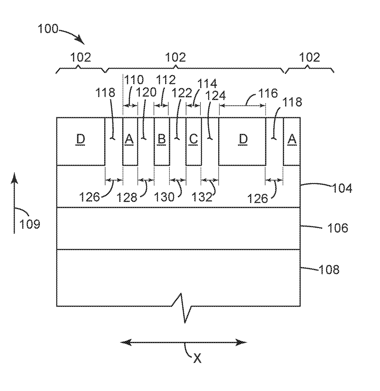
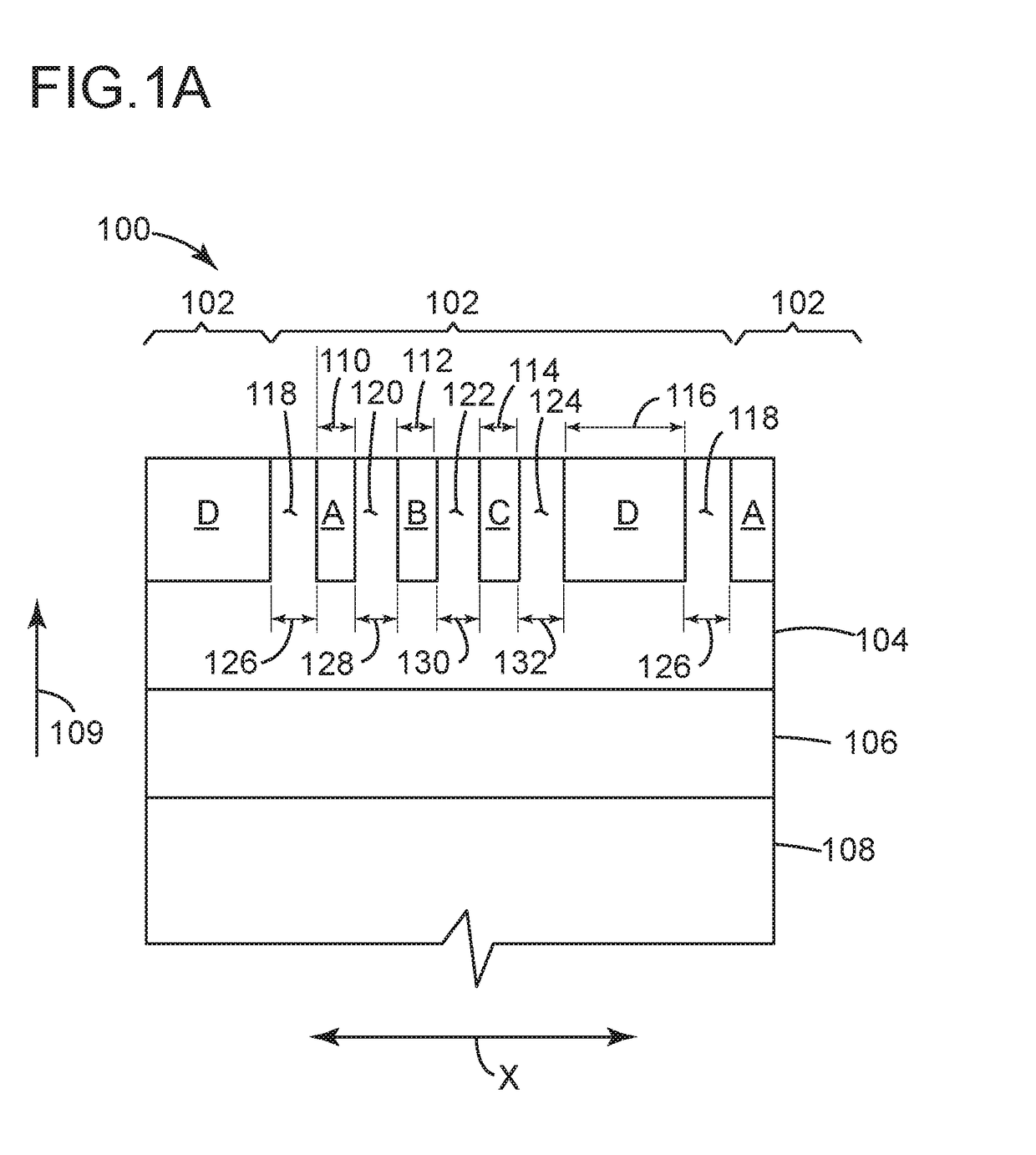
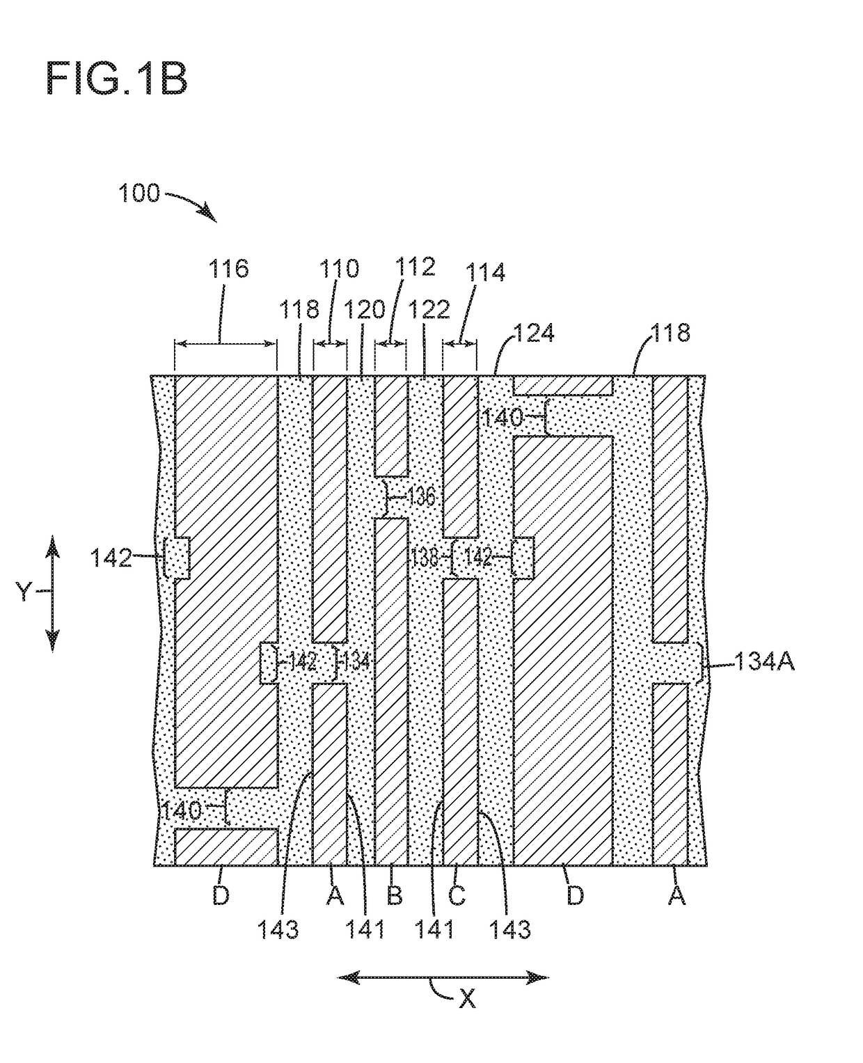
[0057]FIGS. 1A-31 illustrate various exemplary embodiments of an apparatus, and method of making the same, of cells of an interconnect system for a semiconductor structure, wherein...


PUM


Abstract

A semiconductor cell includes a dielectric layer. An array of parallel metal lines is disposed in a longitudinal direction within the dielectric layer. The metal lines having line widths that are substantially equal to or greater than a predetermined minimum line width. Line spacers are disposed between the metal lines. The line spacers having line spacer widths that are substantially equal to or greater than a predetermined minimum line spacer width. The array of metal lines includes a signal line having a continuity cut disposed across its entire line width and a power line adjacent the signal line. The power line has a line width that is greater than twice the minimum line width. The power line has a notch disposed partially across its line width. The notch is aligned with the continuity cut in a direction perpendicular to the longitudinal direction of the metal lines.

Description

CROSS REFERENCE TO RELATED APPLICATIONS[0001]This application is a divisional application of U.S. patent application Ser. No. 15 / 379,740 filed Dec. 15, 2016 entitled, “INTERCONNECTION LINES HAVING VARIABLE WIDTHS AND PARTIALLY SELF-ALIGNED CONTINUITY CUTS.” The above application is incorporated herein by reference in its entirety.TECHNICAL FIELD[0002]The present invention relates to semiconductor devices and methods of fabricating the same. More specifically, the invention relates to a method and apparatus of forming interconnection metal lines having variable pitch and variable line widths for a semiconductor structure.BACKGROUND[0003]Self-aligned multiple patterning (SAMP) techniques (such as self-aligned double patterning (SADP) or self-aligned quadruple patterning (SAQP)) are currently used in ultra-high density integrated circuits to provide an electrical interconnection system which includes multiple arrays of parallel metal lines disposed in several levels of dielectric layer...

Claims


Application Information

Patent Timeline
Patent Type & Authority Applications(United States)
IPC IPC(8): H01L21/768H01L23/528H01L23/522
CPCH01L21/76877H01L23/5286H01L21/76816H01L23/5226H01L23/5283H01L23/528
Inventor LICAUSI, NICHOLAS VINCENTBOUCHE, GUILLAUME
Owner GLOBALFOUNDRIES U S INC
Why Eureka
Try Eureka